
What is a PCB Prototype?
A PCB prototype is an initial version of a printed circuit board designed to validate and test electronic device designs before mass production. It serves a crucial role in various industries such as consumer electronics, telecommunications, automotive, aerospace, medical, and industrial automation by allowing engineers to evaluate functionality, performance, and reliability. PCB prototypes help identify and resolve potential issues early in the development process, minimizing risks and reducing costs associated with design flaws. They enable thorough testing of electronic circuits, components, and systems under real-world conditions, ensuring that the final product meets required specifications and standards. Ultimately, PCB prototypes accelerate time-to-market for new products while ensuring they are of high quality, reliable, and efficient in their intended applications.
PCB Prototype
ISO 9001:2015 | AS9100 Rev. D Certified | IPC-A-610 CLASS 1-2-3 | J Std 001E Class I, II, and III
Technotronix excels in providing comprehensive PCB prototyping services, leveraging advanced techniques such as automated layout analysis, algorithms, and custom technical specimens tailored to Gerber files and Bill of Materials (BOM) specifications. A PCB prototype serves as a fundamental sample for testing design ideas and functionalities, and our extensive experience allows us to deliver prototypes within a remarkable 24-hour turnaround time.
We prioritize client requirements and product quality, ensuring that our quick-turn custom prototype circuit board services are completed within specified timelines. Rigorous full-fledged inspection systems and pre-production checks guarantee the highest standards of quality.
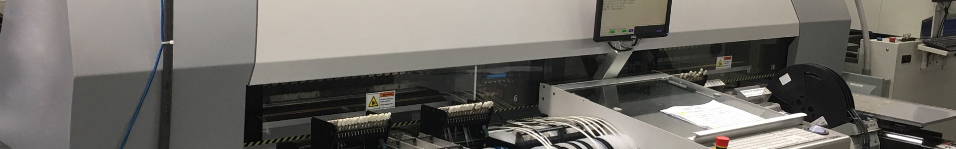
Our capabilities extend to delivering multilayered quick-turn prototypes, incorporating surface mount technology (SMT), chip-on-board (COB), comprehensive testing, and custom PCB prototypes. We cater to diverse industrial sectors including Defense, medical, electronics, renewable energy, and telecommunications, among others.
At Technotronix, we offer flexibility in providing full, partial turnkey, and consigned PCB assembly services alongside custom prototyping solutions. Addressing challenges related to low volume and highly complex assemblies, we employ flying probe testing to detect missing components and validate component placements with precision.
As a leading PCB manufacturing company in California and one of the top printed circuit board manufacturers in the USA, we are committed to delivering superior quality and service. Our expertise in PCB prototype and assembly ensures that every project meets stringent industry standards and exceeds client expectations. Partner with Technotronix for reliable, innovative solutions that drive your product development forward with efficiency and excellence.
Choose Technotronix for your PCB Prototype needs in the USA and California. Our commitment to quality, innovation, and customer satisfaction ensures that you receive the best solutions for your electronic requirements.

Capabilities of Printed Circuit Board Prototypes

PCB Prototype service - 2 layers
Tin Lead Reflow (or Silver) (or Gold) No Silkscreen No Solder mask 23 Preset Drill Sizes up to 200pc PCB prototype

PCB Prototype service - 2,4 and 6 layers
SMOBC (HAL) (or Lead Free Silver) (or Gold) + Silkscreen + Soldermask 23 to 24 Preset Drill Sizes up to 200pc PCB prototype
Other Capabilities
| ITEM | DESCRIPTION |
|---|---|
| Board Thickness | 0.4mm to 2.4 mm |
| Board Dimensions | As per Requirement |
| Min. Hole Size | 0.2mm to 0.3mm |
| Copper Thickness | 35μm, 70μm, 105μm |
| Solder Mask Color | As per Requirement |
| Silk Screen Color | Black, White |
| Controlled Impedance | 25 Ω to 120 Ω |
| Kapton tape thickness | 0.07 mm |
| Angular ring (minimum) | Available |
| Drill file | Depends on the circuit design |
| Press-fit hole | Depends on the design |
| Gold Fingers | Available |
| UL and date code marking | Available |
Preset Board Features
- 2-6 layers up to 200pc.
- Industry standard 0.062" FR-4 laminate.
- Standard 1oz. finished copper weight.
- Minimum trace & space to guarantee manufacturability .006 Inch.
- Smallest board dimension .35 inch in one direction; (square board = .64 x .64.)
- Maximum board size is 12 x 14 (to 168 sq-inches)
- Tin lead or Silver finish or Gold finish
- 24 drill sizes available (finished size after plating):.008, .014, .020, .025, .029, .033, .036, .040, .043, .046, .053, .061, .067, .080, .087, .093, .100, .110, .125, .141, .151, .167, .193, .251 (.008 available with 4 and 6 layer only)
- Green soldermask over bare copper (SMOBC) Hot Air Level (HAL).
- 1 or 2 sided silkscreen (also known as "legend" or "nomenclature").
Lead-Free RoHS compliant PCB prototyping option is available on every service type with no additional lead-time or no additional costs!
PCB Prototyping Process
DFM Review
In DFM review, our engineering team will identify end-of-life (EOL) components if any, layout enhancements, and opportunities to increase efficiency. The purpose of this process is to resolve any potential manufacturing issues immediately.
Material, Components selection and Kit Prep
Our team will work on material and components gathering from trusted suppliers and vendors, guaranteeing quality.
Board Fabrication
In this stage, we will review Gerber files received from customers to kick start the PCB fabrication process.
Assembly & Test
At our manufacturing unit, the prototype specialist assigned to your project goes to your board through each step. From there, the process will continue for the fast-track process, silk screen, soldering, guiding your board through inspection and testing.
Completed Prototype Product Delivery
With our quick NPI process, your PCB prototype product will be delivered with required documentation packages, test certificates (if applicable), and other components if any.
Why Choose Technotronix as PCB Prototype Manufacturer Company?
- Over 44 Years of Experience: With more than 44 years of expertise, we deliver top-notch printed circuit board prototyping services in the USA and California.
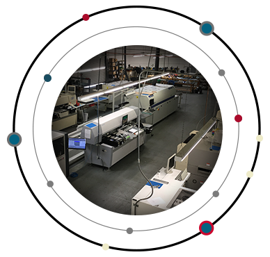
- State-of-the-Art Facility: Our advanced manufacturing unit in California is equipped to produce printed circuit boards, assemble components, and build prototypes efficiently.
- Cost-Effective Mass Production: Our in-house testing ensures that customers receive cost-effective mass production of PCB prototypes.
- Efficient Design Testing: Our team thoroughly tests the overall design, quickly identifying and resolving issues to save costs and time, ensuring the final product performs efficiently.
- Quality Management System: We adhere to the ISO 9001:2015 quality management system, providing standard and quality services that meet PCB prototype requirements for various industries such as electronics, medical, and telecommunications.
- Versatile Project Handling: Whether you need low-volume or high-volume PCB prototype services for over 10,000 pieces, we handle all types of projects.
- Advanced PCB Prototype Capabilities: Utilizing the latest technologies, we guarantee that our customers receive exactly what they want, precisely when they need it.
- Lead-Free and RoHS-Compliant Options: We offer lead-free, RoHS-compliant PCBs based on customer requirements.
- Client Satisfaction: Client satisfaction is our primary goal! We prioritize security and safety concerns, implementing solutions that adhere to industrial standards and guidelines.
Our comprehensive PCB prototype service encompasses printed circuit board prototype, PCB manufacturing and assembly, and printed circuit board manufacturing. We ensure your project benefits from our extensive experience and commitment to quality, delivering reliable and efficient solutions for all your PCB prototype and assembly needs. Choose Technotronix for your PCB Prototype needs in the USA and California, and experience the benefits of working with an industry leader dedicated to innovation and excellence.
PCB Prototype Services for various industries
Our PCB prototyping services serve several critical industrial applications. Here are some key industrial applications:
Electronics and Consumer Goods
Telecommunications
Energy and Utilities
Automotive
Aerospace and Defense
Medical Devices and Healthcare
Industrial Automation
FAQs
Different methods of PCB prototyping includes:
- Etching: Using chemicals to remove copper from a copper-clad substrate.
- CNC Milling: Cutting away copper using a computer-controlled machine.
- 3D Printing: Building up layers of conductive or insulating material to create the circuit.
- Inkjet Printing: Depositing conductive ink onto a substrate using an inkjet printer.
- Laser Direct Structuring (LDS): Using a laser to activate a surface for subsequent metallization.
For more information check out
Our Most Recent and PCB Prototypes Related Articles
Do you have any PCB Prototype requirements? Request a free PCB Prototype quote. Alternatively, email BoM, Gerber files, and other required details at [email protected] or call us 714/630-9200.

PCB Assembled in 24 hours
Kitted and Turn-Key option as per customers requirement.
REQUEST OUR BROCHURE
 Request Brochure
 Please provide your email address. We’ll send you copy of our brochure in a PDF format.