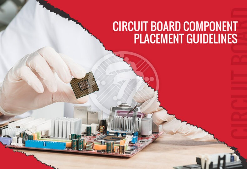
Top Circuit Board Component Placement Guidelines

With miniaturization becoming the order of the day, the one thing that is becoming extremely complex is PCB layout. Not only does it have to cater to reduced space but also to increased functional requirements. Besides, with high-speed circuitry what is needed is layout precision so that there are no issues related to signal integrity or to do with effective heat dissipation.
Therefore, the important thing is to balance the manufacturing requirements along with the circuit board component placement requirements. Some of the other factors that need to be kept in mind include the fact that at the time of testing, there needs to be accessibility of parts.
Functional needs of the circuitry
- The process needs to begin with floor planning. You need to figure out where you will place the digital, analog, RF & power areas. It is imperative that these areas are kept isolated so that signal integrity is maintained.
- Fixed components such as connectors must be placed first.
- While transitional components can infringe into other areas, the rest of the components should not.
- Ensure that the routing channels aren’t choked and that there is space for escape & bus routing. It is also important to ensure clear return paths and therefore vias should not block the signal return paths.
- The components of high-speed signals should be placed close together & the connections need to be short.
- The components of power supply need to be placed close together. Additionally, power supply components should be placed on the same layer. This ensures that there is no need for any vias.
- Components that generate heat such as processors, need to be placed towards the center of the board so that there is efficient heat dissipation. You also need to be careful about the management of the airflow. Proper placement of heat sinks and other heat dissipation devices is also important.
Circuit Board Component Placement for Manufacturing
- For SMT parts that cannot be wave soldered, ensure that there is extra clearance available. That way you will be able to mask these SMT parts.
- Components that can be wave soldered should have their pins perpendicular to the direction of travel through the wave.
- In terms of component size, small SMT components should not be directly placed behind the large components.
- Through-hole connectors need to be oriented in such a manner that their pins travel perpendicular to the wave.
- Tall components should not be placed on the back of the board.
Circuit Board Component Placement for Accessibility
- At the testing stage it is important that there be access to the board in terms of plugging in cables, attaching wire clips & more.
- PCB layout needs to take into account the fact that wire harnesses have to be fixed, batteries have to be replaces & more. The layout, therefore, needs to allow accessibility for this.
- Component placement also needs to take into account the fact that intra-system connections may need to go through a redesign.
- The circuit board needs to be designed in a manner that test points are designed into it. Test points, in turn, have their own specific requirements when it comes to placement. Some of the aspects to take care of include test point to test point spacing, test point to component spacing, and test point to board edge spacing.
- The arrangement of the board in the manufacturing panel also impacts the placement of components. For panels that use a scoring tool for separation, due care needs to be taken to see that components have enough clearance from the edge. Similarly, the panels that use break-out tabs need to ensure that the components are kept away from the tabs.
- In cases where the board is conformally coated, it is worth remembering that unique components are placed at the edge so that they do not dip in the coating.
To sum up
To avoid functional and manufacturing problems in your design, The circuit board components need to be placed considering a wide variety of factors such as:
- Functional Requirements
- Manufacturing Requirements
- Accessibility of parts
Due consideration given to each of these aspects ensures that the PCB works as planned and that there are no costly issues to contend with at a later stage.
Technotronix provides a one-stop solution for electronics manufacturing services with specialized support, reliable testing, and multi-functional features. In case if you have any questions, please feel free to contact us via email at [email protected] or call us at 714/630-9200.


