Enhancing Quality Control in Electronics: The Role of Computer Vision in PCB Assembly Inspection

By | Date posted: | Last updated: November 27, 2024
PCB Assembly Inspection

In the world of electronics manufacturing, ensuring the quality of printed circuit board (PCB) assemblies is crucial. As technology evolves and devices become more compact and complex, maintaining high-quality standards has become more challenging. This is where computer vision technology has made a significant impact. By leveraging computer vision for PCB assembly inspection, manufacturers can automate quality control, reduce human error, and achieve faster production times. In this blog, we’ll explore how computer vision is transforming PCB assembly inspection, its benefits, and how it enhances quality control in electronics manufacturing.

PCB assembly is the process of soldering electronic components onto a printed circuit board to create functional electronic devices. It involves placing components like resistors, capacitors, microchips, and connectors onto the PCB using automated machinery. The final product is then tested to ensure functionality before being incorporated into electronic devices such as smartphones, computers, and medical equipment.

What are the challenges in PCB assembly inspection?

PCB assembly is intricate, with even minor defects such as misaligned components, poor solder joints, or tiny cracks potentially leading to device failures. Traditionally, visual inspection of PCBs relied on manual methods, where inspectors used magnifying glasses or microscopes. However, manual inspection is time-consuming and prone to human error, especially with high-volume production. The increasing complexity of PCBs, with their smaller and denser layouts, has amplified these challenges, necessitating advanced solutions like computer vision.

What is computer vision in PCB assembly?

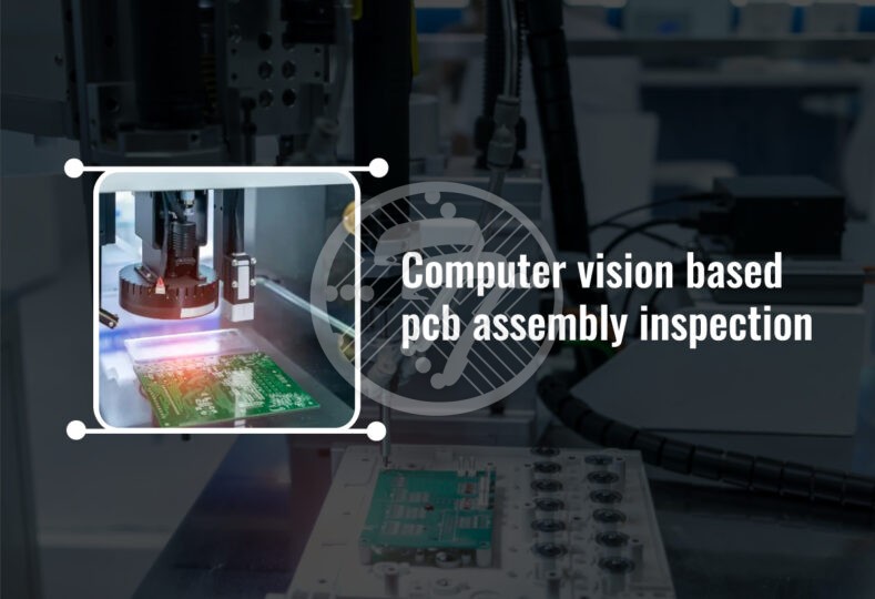
Computer vision is a field of artificial intelligence (AI) that enables computers to interpret and analyze visual data from the world, including images and videos. In electronics manufacturing, computer vision systems use high-resolution cameras and deep learning algorithms to capture and analyze images of PCBs during assembly. This technology automates the inspection process, ensuring that each board meets the required quality standards.

How does computer vision work in PCB inspection?

In PCB assembly inspection, computer vision systems capture images of each board as they move along the production line. Advanced algorithms then analyze these images to detect defects such as missing components, incorrect orientation, poor solder joints, and misalignments. The system compares the inspected board against a reference image of a correctly assembled PCB, identifying any deviations that could affect the performance of the final product.

Benefits of using computer vision for PCB assembly inspection

  1. Enhanced Accuracy and Reliability: Computer vision technology dramatically improves the accuracy and reliability of PCB inspections. Unlike human inspectors, computer vision systems can work consistently without fatigue, ensuring that every board is inspected with the same level of precision. This reduces the risk of errors and helps in identifying defects that may be too small for the human eye to detect.
  2. Faster Inspection Times: With the ability to process thousands of images per minute, computer vision speeds up the inspection process, allowing manufacturers to maintain high production rates without compromising quality. This is particularly important in industries like consumer electronics, where time-to-market is a critical factor.
  3. Cost Reduction Automating PCB inspection with computer vision helps manufacturers reduce labor costs associated with manual inspections. Additionally, the early detection of defects prevents defective boards from progressing further down the production line, saving costs on rework and minimizing waste.
  4. Real-time Monitoring and Data Collection: Computer vision systems can provide real-time monitoring of PCB assembly lines, allowing for immediate identification and correction of issues. The data collected during inspections can be analyzed to identify recurring defects or process inefficiencies, enabling manufacturers to continuously improve their production processes.
  5. Improved Product Quality and Customer Satisfaction: By ensuring that every PCB meets strict quality standards, computer vision enhances the overall quality of electronic products. This leads to fewer returns and warranty claims, resulting in improved customer satisfaction and brand reputation.

Key applications of computer vision in PCB assembly inspection

  1. Automatic Optical Inspection (AOI): is one of the most common applications of computer vision in PCB manufacturing. AOI systems use high-resolution cameras and sophisticated algorithms to inspect PCBs for defects such as misaligned components, missing parts, and soldering issues. AOI systems can inspect boards at different stages of production, including pre-reflow (before soldering) and post-reflow (after soldering), ensuring that any issues are identified and corrected promptly.
  2. Solder Paste Inspection (SPI): Solder paste inspection (SPI) is another critical area where computer vision is used. During PCB assembly, solder paste is applied to the board before components are placed. Any inconsistencies in the thickness or placement of solder paste can lead to poor solder joints and, ultimately, faulty products. Computer vision-based SPI systems analyze the application of solder paste, ensuring that it meets the required specifications before components are placed.
  3. 3D Imaging for Complex Defect Detection: Computer vision systems can also incorporate 3D imaging to inspect PCBs with complex geometries. By analyzing 3D images of the board, these systems can detect defects that might be hidden in 2D images, such as component tilt or insufficient solder volume. This added dimension provides a more comprehensive view of the assembly, further improving defect detection accuracy.

Implementing computer vision in PCB Assembly: Challenges and considerations

  1. High Initial Investment: One of the primary challenges in implementing computer vision systems is the high initial cost of hardware, software, and integration into existing production lines. However, the long-term benefits of improved quality control and reduced waste often outweigh these initial expenses.
  2. Need for Expertise: Integrating computer vision into PCB assembly requires expertise in both electronics manufacturing and AI-based image analysis. Manufacturers may need to train staff or work with specialized vendors to ensure proper implementation and maintenance of the system.
  3. Adapting to Changing Product Designs: PCB designs can change frequently due to evolving product specifications. Computer vision systems must be adaptable, with algorithms that can be updated or trained to accommodate new board designs. Flexibility is key to maintaining effective quality control across different product lines.
  4. Data Security and Privacy Concerns: As computer vision systems collect and analyze large volumes of data, manufacturers must ensure that this data is stored securely and in compliance with data privacy regulations. This is particularly relevant when working with sensitive designs or in industries like defense and medical devices.

Conclusion

Computer vision has revolutionized the way PCB assembly inspections are conducted, offering unparalleled accuracy, speed, and efficiency. By automating the inspection process, manufacturers can achieve higher quality standards, reduce costs, and accelerate production times. As technology continues to advance, the role of computer vision in PCB manufacturing will only grow, making it an indispensable tool for quality control in the electronics industry. For manufacturers looking to stay competitive in a fast-paced market, investing in computer vision solutions is a strategic move toward ensuring the highest standards of product quality.

Ready to elevate your product quality? At TechnoTronix, we specialize in PCB assembly services backed by advanced computer vision inspection to ensure top-tier quality control at every stage. With our cutting-edge technology, we detect defects early, optimize production, and deliver reliable, high-performance electronics. Contact us today to discuss how we can support your next project with precision and innovation in PCB assembly!

PCB assembly for electric vehicles: Meeting the growing demand for high-performance electronics!

By | Date posted: | Last updated: October 23, 2024
PCB Assembly for Electric Vehicles

The electric vehicle (EV) market is experiencing unprecedented growth, driven by a global push toward sustainable transportation and the urgent need to reduce carbon emissions. Central to the performance and reliability of EVs are the electronic systems that control everything from battery management to infotainment. At the heart of these systems are printed circuit boards (PCBs), which play a crucial role in ensuring the efficient operation of EVs. This article explores the importance of PCB assembly in electric vehicles and how manufacturers are rising to meet the growing demand for high-performance electronics.

The Role of PCBs in Electric Vehicles

PCBs are the backbone of electronic devices, providing the physical platform for mounting and interconnecting various electronic components. In electric vehicles, PCBs are used in a wide range of applications, including:

  • Battery Management Systems (BMS): The BMS monitors and manages the state of the battery, ensuring optimal performance and safety. This system involves complex circuitry that requires high-quality PCBs to handle power and data signals efficiently.
  • Power Electronics: These include inverters, converters, and chargers that manage the flow of electricity between the battery and the motor. High-performance PCBs are essential for handling the high currents and voltages involved.
  • Infotainment Systems: Modern EVs are equipped with advanced infotainment systems providing navigation, entertainment, and connectivity features. These systems rely on PCBs to integrate various functions seamlessly.
  • Advanced Driver Assistance Systems (ADAS): Technologies such as adaptive cruise control, lane-keeping assist, and collision avoidance require reliable PCBs to process data from sensors and cameras in real-time.

Challenges in PCB Assembly for EVs

The assembly of PCBs for electric vehicles presents several unique challenges:

  • Thermal Management: EVs generate significant heat, especially within power electronics like inverters, converters, and motor controllers. Effective thermal management is crucial to prevent overheating, which can lead to component failure or reduced efficiency. Manufacturers must use materials with high thermal conductivity, such as copper and aluminum substrates, to dissipate heat efficiently. Advanced cooling techniques, including heat sinks, thermal vias, and liquid cooling systems, are also employed to maintain optimal temperatures. Additionally, managing the thermal expansion coefficients between different materials is critical to prevent stress and damage during temperature fluctuations.
  • High Reliability: Electric vehicles often operate in challenging environments that involve vibrations, rapid temperature changes, humidity, and exposure to dust and contaminants. These harsh conditions demand that PCBs are highly reliable and durable. To meet these requirements, manufacturers must follow strict quality standards such as IPC-A-600 for PCB fabrication and IPC-A-610 for assembly. Advanced protective measures, like conformal coatings and encapsulation, are used to shield sensitive components from moisture and contaminants. Rigorous testing protocols, including temperature cycling, vibration testing, and humidity testing, ensure that the PCBs can withstand the demands of real-world EV applications.
  • Miniaturization: As EVs become more compact and feature-rich, there is a growing need for miniaturized PCBs that can fit into smaller spaces without compromising performance. This miniaturization requires advanced manufacturing techniques, such as HDI (High-Density Interconnect) PCBs, which allow for finer traces, microvias, and increased layer counts. Precision engineering ensures that even the smallest components are placed accurately to maintain signal integrity and power distribution. Designers also leverage 3D PCB design software to optimize the layout, reducing the overall footprint while accommodating the necessary functionality.
  • High Power Density: The power requirements of EVs are significantly higher than those of conventional vehicles, due to the high energy demands of the battery, motor, and power management systems. PCBs must be designed to handle high power densities, with thicker copper layers and wide traces to support the flow of large currents without overheating. Techniques like impedance matching and careful power plane design are essential to ensure stable power delivery and minimize losses. Effective grounding and shielding methods are also critical to reducing electromagnetic interference (EMI), which can affect the performance of high-power circuits. Additionally, high-power designs require careful consideration of voltage isolation and creepage distances to maintain safety standards, especially in applications where high voltages are present.
  • Cost and Scalability: As the EV market grows, manufacturers must balance the need for high-performance PCBs with the pressure to reduce costs and maintain scalability. The production of advanced PCBs can be costly, especially when using high-end materials and sophisticated assembly processes. To achieve cost efficiency, manufacturers often invest in automation, such as automated optical inspection (AOI) and surface mount technology (SMT) pick-and-place machines, to minimize labor costs and improve consistency. However, scaling up production while maintaining quality can be challenging, especially with the rapidly evolving technology landscape in the EV industry. This makes it essential for manufacturers to strike a balance between innovation, cost management, and production scalability.
  • Compliance with Industry Standards: EV manufacturers must adhere to a range of industry standards and regulations that govern the design, manufacturing, and testing of electronic components. Standards such as ISO 16750 (environmental conditions and testing for electrical and electronic equipment in road vehicles) and IPC standards for PCBs ensure the safety and performance of the electronics used in EVs. Compliance with these standards can be complex and time-consuming, requiring thorough documentation and validation processes. Manufacturers must stay updated on evolving regulations and adjust their processes to remain compliant, ensuring that their PCBs meet the safety and performance criteria set by automakers and regulatory bodies.

Innovations in PCB Assembly for EVs

To meet the growing demand for high-performance electronics in electric vehicles, manufacturers are adopting several innovative approaches:

  • Advanced Materials: The use of advanced materials, such as high-temperature laminates, metal core PCBs, and ceramic substrates, improves thermal management and reliability. These materials can withstand higher temperatures and provide better heat dissipation.
  • Automated Assembly Processes: Automation in PCB assembly, including surface mount technology (SMT) and automated optical inspection (AOI), ensures high precision and consistency. This reduces the risk of defects and improves overall quality.
  • Flexible PCBs: Flexible PCBs, also known as flex circuits, offer greater design flexibility and can be bent or folded to fit into tight spaces. They are increasingly used in EVs to connect different modules and components, maximizing space efficiency.
  • Embedded Components: Embedding passive and active components within the PCB substrate can reduce the overall size and weight of the board. This approach improves electrical performance by minimizing signal loss and interference.
  • Advanced Testing and Inspection: Rigorous testing and inspection processes, including X-ray inspection, thermal imaging, and functional testing, are essential to ensure the reliability and performance of PCBs. Manufacturers are investing in advanced testing equipment to detect and address potential issues early in the production process.

The Future of PCB Assembly in Electric Vehicles

The future of PCB assembly for electric vehicles looks promising, with several trends shaping the industry:

  • Integration of AI and IoT: The integration of artificial intelligence (AI) and the Internet of Things (IoT) in EVs will drive the demand for more sophisticated PCBs. These technologies require advanced processing capabilities and connectivity, enabled by high-performance PCBs.
  • Sustainability: As the EV industry focuses on sustainability, there is a growing emphasis on environmentally friendly PCB manufacturing processes. This includes the use of lead-free solder, recyclable materials, and energy-efficient production methods.
  • Customization: The increasing diversity of EV models and applications will drive the demand for customized PCBs. Manufacturers will need to offer tailored solutions to meet the specific requirements of different EV platforms.
  • Collaboration and Standardization: Collaboration between automakers, electronics manufacturers, and standards organizations will be crucial in developing industry-wide standards for PCB design and assembly. Standardization will help streamline production processes and ensure compatibility across different systems.

Conclusion

The rapid growth of the electric vehicle market presents both opportunities and challenges for PCB assembly. As the demand for high-performance electronics continues to rise, manufacturers must innovate and adapt to meet the evolving needs of the industry. By leveraging advanced materials, automated processes, and rigorous testing, they can ensure the reliability and efficiency of PCBs in electric vehicles. The future of PCB assembly in EVs is bright, with ongoing advancements promising to drive further improvements in performance, sustainability, and customization.

As we move toward a more electrified future, understanding the role of PCBs will be essential for anyone interested in the EV industry. Staying informed about the latest technologies and trends in PCB assembly can help industry professionals and enthusiasts alike contribute to this exciting and rapidly evolving field.

At Technotronix, we specialize in delivering cutting-edge PCB assembly services tailored for electric vehicles. Our advanced manufacturing capabilities ensure high-performance electronics that meet the rigorous demands of the EV industry. Whether it’s optimizing efficiency or enhancing reliability, we’re here to support your journey towards innovative mobility. Request a PCB assembly quote today to discuss your EV PCB assembly requirements and discover how we can help you stay ahead in the rapidly evolving electric vehicle market.

What are the specific requirements of Bill of Materials (BOM) for cable harness assembly manufacturing?

By | Date posted: | Last updated: August 15, 2024
BOM for Cable Harness Assembly

In the manufacturing of cable harness assemblies, the Bill of Materials (BOM) is a critical document that details all the components, materials, and assemblies required to produce a final product. An efficient and cost-effective manufacturing process relies on a well-structured BOM. It provides a comprehensive guide for sourcing materials, managing inventory, and facilitating communication between different departments. This article will explore the specific requirements of a BOM needed for cable harness assembly manufacturing, highlighting its importance and key components.

The importance of a BOM in cable harness assembly

A BOM is more than just a list of parts; it is a comprehensive document that provides detailed information about each component required for the manufacturing process. This detailed document acts like a recipe, outlining the exact specifications and quantities of materials needed, much like a recipe provides the ingredients and instructions for baking cookies. A BOM serves multiple purposes in the manufacturing of cable harness assemblies:

  • Material Management: It lists all materials required, helping to maintain optimal inventory levels and avoid shortages or excesses.
  • Cost Estimation: By detailing all components and quantities, a BOM aids in accurate cost calculation, which is crucial for pricing and budgeting.
  • Production Planning: It provides a blueprint for the assembly process, ensuring that all necessary parts are available, and that the assembly can proceed without interruptions.
  • Quality Control: A BOM helps ensure that the correct components are used, maintaining the quality and consistency of the final product.
  • Regulatory Compliance: In industries with stringent regulations, a BOM helps ensure that all materials and processes comply with relevant standards

Key Components of a BOM for Cable Harness Assembly

A BOM for cable harness assembly manufacturing typically includes several key components:

  1. Part Number: A unique identifier for each component, which simplifies tracking and management.
  2. Description: A detailed description of each component, including specifications such as dimensions, materials, and electrical properties.
  3. Assembled quantity: The number of components required.
  4. Unit of Measure: The measurement unit used to quantify each component (e.g., pieces, meters).
  5. Manufacturer’s Part Number: The part number assigned by the component’s manufacturer, who helps in sourcing and verification.
  6. Supplier Information: Details of the suppliers from whom the components can be sourced, including contact information and lead times.
  7. Component Image: Visual representation of each component, which aids in identification and assembly.
  8. Assembly Instructions: Specific instructions on how each component should be assembled, including any special handling or installation requirements.

Detailed Requirements for Cable Harness Assembly BOM

To create an effective BOM for cable harness assembly, certain specific requirements need to be met:

  1. Comprehensive Component Listing

    A cable harness assembly BOM must include all components, no matter how small or seemingly insignificant. This includes:

    • Wires and Cables: Detailed information on wire types, lengths, gauges, and insulation materials.
    • Connectors: Specifications for connectors, including type, pin configuration, and mating requirements.
    • Terminals: Types of terminals used, their material, and crimping specifications.
    • Protective Components: Items such as sleeves, grommets, and heat shrink tubing, including their sizes and materials.
    • Mounting Hardware: Details of any brackets, clamps, or fasteners required to secure the harness in place.
    • Labels and Markers: Information on labeling and marking components for identification and compliance purposes.
  2. Material Specifications

    For each component, the BOM should include precise material specifications. This ensures that the correct materials are used, which is crucial for performance, safety, and compliance. Material specifications should cover:

    • Electrical Properties: Conductivity, resistance, and insulation ratings.
    • Mechanical Properties: Tensile strength, flexibility, and durability.
    • Environmental Resistance: Resistance to factors such as temperature, moisture, chemicals, and UV exposure.
  3. Quantities and Units of Measure

    Accurate quantities and appropriate units of measure are essential for effective material management. The BOM should specify the exact number of each component needed, along with the unit of measure (e.g., meters for cables, pieces for connectors). This helps in precise inventory management and cost estimation.

  4. Source and Supplier Details

    To streamline procurement, the Bill of Materials (BOM) should include detailed information about the sources and suppliers of each component. This should cover:

    • Supplier Names: Names of approved suppliers for each component.
    • Contact Information: Contact details for procurement and order placement.
    • Lead Times: Estimated lead times for each component, which aids in production planning.
    • Alternative Suppliers: Information on alternative suppliers in case of supply chain disruptions.
  5. Assembly Instructions and Quality Control

    The BOM should include detailed assembly instructions to guide the manufacturing process. This ensures that components are assembled correctly and efficiently. Additionally, quality control checks should be integrated into the instructions, specifying:

    • Inspection Points: Key stages in the assembly process where quality checks are required.
    • Testing Requirements: Electrical and mechanical tests that need to be performed on the assembled harness.
    • Acceptance Criteria: Standards and criteria that the final product must meet to be considered acceptable.
  6. Regulatory and Compliance Information

    In industries such as automotive, aerospace, and medical devices, regulatory compliance is critical. The BOM should include information on relevant standards and regulations, ensuring that all components and processes comply. This may cover:

    • Safety Standards: Compliance with electrical and fire safety standards.
    • Environmental Regulations: Adherence to regulations on hazardous materials (e.g., RoHS, REACH).
    • Industry-Specific Standards: Compliance with industry-specific standards (e.g., IPC/WHMA-A-620 for cable and wire harness assemblies).

Future Trends in BOM Management

As technology evolves, so do the tools and methods for managing BOMs. Innovations such as flexible PCBs, High-Density Interconnect (HDI) technology, and substrate-like PCBs (SLP) are changing the landscape of cable harness manufacturing. These advancements allow for smaller, more efficient designs, which in turn require more precise and detailed BOMs.

Additionally, the use of Internet of Things (IoT) and Artificial Intelligence (AI) in manufacturing is enhancing the accuracy and efficiency of BOM management. AI can help identify potential issues before they arise, while IoT enables real-time tracking of components and materials.

Sustainability in Cable Harness Manufacturing

Sustainability is becoming increasingly important in manufacturing. Innovative materials, such as water-soluble PCBs like Soluboard, are reducing waste and environmental impact. As manufacturers strive to meet sustainability goals, BOMs will play a critical role in ensuring that materials and processes align with these objectives.

Conclusion

A comprehensive and detailed BOM is indispensable for the successful manufacturing of cable harness assemblies. It ensures that all necessary components are accounted for, facilitates efficient production planning, and helps maintain high-quality standards. By including all relevant information—such as part numbers, descriptions, quantities, material specifications, supplier details, assembly instructions, and regulatory compliance—the BOM becomes a crucial tool in the manufacturing process. Properly managed, a BOM not only streamlines operations but also contributes to cost savings, improved quality, and enhanced overall efficiency in cable harness assembly manufacturing.

At Technotronix, we have more than 40 years of experience in manufacturing and assembling industry-leading products. Equipped with state-of-the-art equipment and skilled personnel, we offer products to meet your requirements. TechnoTronix is a leading cable and wire harness assembly manufacturer who will deliver ample of smart solutions related to PCBs.

In-Circuit Testing (ICT) vs Functional testing in PCB assembly – When to use?

By | Date posted: | Last updated: December 10, 2024
In-circuit Test vs Functional Test

In the world of printed circuit board (PCB) assembly, testing plays a crucial role in ensuring the quality and functionality of the final product. Two common testing methods used are In-Circuit Testing (ICT) and Functional Testing (FCT). While both aim to identify defects and faults in the PCB assembly, they differ in their approach and scope. In this article, we will explore the differences between ICT and functional testing and discuss when to use each method.

What is in-circuit testing (ICT)?

In-Circuit Testing is a method used to test electronic components and connections on a PCB to ensure their proper functioning. It is typically performed early in the manufacturing process to detect and rectify any issues before delivering defective products to customers. ICT involves connecting the PCB to specialized testing equipment that places test probes or pins at critical test points on the board. These probes measure various parameters such as resistance, capacitance, inductance, and shorts. Additionally, ICT checks that electronic components are correctly installed and connected.

This testing method involves measuring and testing the individual components on a PCB. It is performed by connecting the PCB to specialized testing equipment, which places test probes or pins at key test points on the board. These probes measure parameters such as resistance, capacitance, inductance, and shorts. The primary goal of ICT is to identify manufacturing defects, such as open connections, solder shorts, and incorrect or missing components.

ICT is designed to catch manufacturing defects, open connections, solder shorts, and incorrect or missing components on a PCB. It provides a comprehensive check of the circuit, detecting power and ground shorts in a relatively short period of time. The testing process is controlled by specialized software, which allows for accurate measurements and reduces the risk of misjudgment. With ICT, manufacturers can identify which part or circuit is connected, making it easier to troubleshoot and maintain the PCB assembly. This not only speeds up the production process but also improves product quality.

What are the advantages of ICT?

There are several advantages to using ICT in PCB assembly testing:

  • Detection of Manufacturing Defects: ICT can quickly identify defects in the PCB assembly, ensuring that the final product meets the required quality standards.
  • Fast and Accurate Testing: ICT is known for its speed and accuracy. The testing process can be completed in a matter of seconds, allowing for efficient testing of large volumes of PCB assemblies.
  • Computer-controlled Testing: ICT is controlled by a computer program, which ensures accurate measurements and reduces the risk of misjudgment or missed measurements.
  • Facilitates Maintenance and Troubleshooting: ICT provides valuable information about the connectivity of different parts or circuits on the PCB. This information can be used for maintenance purposes and to speed up the production process.

What are the disadvantages of ICT?

While ICT has its advantages, there are also some limitations to consider:

  • Limited Scope: ICT focuses on individual component testing and may not provide a comprehensive evaluation of the overall functionality of the PCB assembly.
  • High Upfront Costs: Setting up an ICT system requires specialized equipment and expertise, which can be expensive initially.
  • Inability to Test Certain Components: ICT may not be suitable for testing components that require power or specific environmental conditions to function properly.

What is functional testing (FCT)?

Functional testing (FCT) is a testing method that evaluates most of the normal operating functionality of the PCB assembly. Unlike ICT, which focuses on individual components, FCT however rarely ensures that the PBCA can function as expected when abnormal events arise, unless special precautions have been taken in the design and test stages. This testing method simulates the operating environment of the device under test (DUT) and checks for various functional parameters such as voltage, current, power, power factor, frequency, and duty cycle.

What are the advantages of FCT?

Functional testing offers several advantages in the PCB assembly process:

  • Comprehensive Evaluation: FCT provides a holistic evaluation of the PCB assembly’s functionality, ensuring that all components work together as intended.
  • Real-world Simulation: FCT simulates the operating conditions of the PCB assembly, allowing manufacturers to test its performance under realistic scenarios.
  • Cost-effective Testing: By testing the entire PCB assembly, FCT can identify potential issues that may arise from the interaction of different components, reducing the need for expensive system-level testing.
  • Improved Product Quality: FCT helps to identify any design or manufacturing flaws that may affect the performance or reliability of the PCB assembly, leading to improved product quality.

What are the disadvantages of FCT?

Despite its advantages, FCT also has some limitations:

  • Time-consuming Testing: FCT typically requires more time compared to ICT due to the comprehensive nature of the testing process.
  • Higher Complexity: FCT requires specialized equipment and expertise to set up and execute properly, which can increase the complexity of the PCB assembly process.
  • Limited Fault Detection: While FCT can identify functional issues, it may not detect certain manufacturing defects or component-level faults that ICT is capable of catching.

When to use ICT and functional testing?

Both ICT and functional testing have their strengths and weaknesses, making them suitable for different stages of the PCB assembly process. Here are some scenarios where each testing method can be beneficial:

When to use ICT?

  • Use ICT when you need to identify manufacturing defects, such as open connections, solder shorts, or missing components.
  • ICT is valuable for testing large volumes of PCB assemblies quickly and accurately.
  • When you need to ensure the connectivity of different parts or circuits on the PCB for maintenance and troubleshooting purposes, ICT can provide valuable insights.

When to use functional testing?

    • Use FCT when you need to evaluate the overall functionality and performance of the PCB assembly as a whole.
    • FCT is ideal for simulating real-world operating conditions and testing the interaction of different components.
    • When you want to ensure that the PCB assembly meets the required functional parameters and performs as intended, FCT is an essential testing method.

Conclusion

In-Circuit Testing (ICT) and Functional Testing (FCT) are two commonly used methods in PCB assembly testing. While ICT focuses on individual component testing and detecting manufacturing defects, FCT evaluates the overall functionality and performance of the PCB assembly. Understanding the differences between these testing methods is crucial for selecting the appropriate approach based on the specific requirements of your PCB assembly. By leveraging the strengths of ICT and FCT, manufacturers can ensure the quality and reliability of their PCB assemblies in various applications and industries.

Technotronix offers professional PCB assembly and testing services with 44+ years of expertise. Ensure flawless PCB assembly with our comprehensive suite of in-circuit testing (ICT) and functional testing (FCT) services. Let us optimize your electronics manufacturing process for peak performance and reliability that meets the quality standards, including ISO-9001:2015, RoHS, and more. If you have any questions or any requirements related to PCB assembly service, please feel free to contact us via email at [email protected] or request a quote for PCB assembly services!