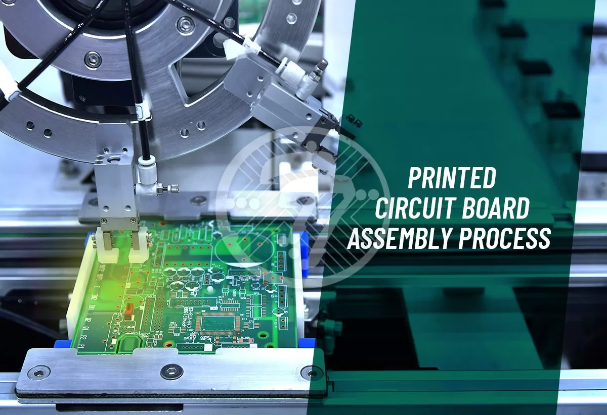
Best Practices to Ensure the Correct Component Orientation by Optimized assembly PCB board!

By | Date posted: | Last updated: September 9, 2024
Assembly PCB Board

A connection is something very important. No one can live in isolation for the entire time. This is not only applicable to living beings. Don’t get confused now. Here we are talking about the components of PCB (Printed-circuit boards). Without proper connections, do you think you would find a working PCB? It’s not possible.

One of the most important parts of making a PCB is its component orientation when talking about PCB. It is not at all possible to make it without a proper component orientation. Now, think of a fast-flowing river, and you have to swim across it. Do you think you can go in the opposite direction of the river’s flow?

Personally, I don’t think it’s quite possible. It will be a lot of effort to go the other way rather than how the river’s water is flowing – component orientation on PCBs. You cannot put it incorrectly, or else Loads of problems will arise.

All this describes how important it is to have the correct component orientation to optimize the Assembly of PCBs. Assembly of printed circuit boards won’t be that difficult if different components’ orientation is in an aligned order and correctly placed.

Why is correct component orientation necessary?

As I’ve already told above, component orientation is necessary for the Printed Circuit Boards Assembly Process. If the components are not in an aligned position, it can create various defects and functional issues after the PCB assembly service. It can lead to poor functionality of the PCB, defects in its services, and many other electrical problems. Thus, correct component orientation is necessary.

Work with the PCB Assembler

For circuit board assembly, professional assistance is crucial. With the help of a PCB board manufacturer, assembly will be more manageable, and component orientation will be precise. A PCB contract manufacturer can ensure that the quality of the parts is high, minimizing time and labor while avoiding assembly issues. Accurate component orientation enhances manufacturability, ensuring your PCB meets specifications.

An experienced PCB assembler is also essential for optimizing printed circuit board manufacturing. They offer valuable expertise on circuit board functionality and assembly requirements, making your efforts more effective. Professional support will significantly benefit the correct component orientation through optimized PCB assembly.

Things to keep in mind before component orientation on Printed Circuit Board Assembly

To make sure that the printed circuit boards assembly is successful, you need to have a correct component orientation. But how can you do that? Well, correct placement and orientation is an important aspect of assembly PCB board.

  • Please do remember the orientation of the components that are similar to each other, which means putting similar components in the same direction. Thus, it can help you get the proper idea of Orienting all the components according to the PCB. Alignment is very important, and the assembly PCB board depends on it.
  • You will have to avoid placing any component on the solder side during the PCB assembly service. It is a crucial thing that you will have to take into consideration. If you don’t, then there might be bad or poor solder joints and electrical function problems.
  • Another thing that you should consider while Assembly of printed circuit boards is the placement of SMT components. You should try and place them on the same side of a PCB. Also, you need to place all the through-hole components on the PCB’s top-side.
  • On having mixed technology components, SMT and PTH, there will be a need for an extra process. the manufacturers might need it for the bottom components’ epoxy.

Manufacturing and functional considerations for PCB components Assembly:

There are two aspects that you should consider during component orientation on a PCB. You should make sure that your PCB is both manufacturable and functional. It is because the manufacturability of your board is important, and so is its functionality. Both of these aspects will decide whether your PCB will be perfectly working or not.

Manufacturable aspect

  • The quality of the parts or materials should not be defective so that the assembly process will be smooth.
  • In waved soldered boards, you should make sure that no components are misaligned as it can lead to various problems during the PCB assembly process.
  • Separation of PCBs from their manufacturing panels is done with the help of V-groves scoring. You should make sure that the parts are oriented and placed so that the scoring tool gets enough place to work.

Functional aspect

  • Certain parts in a PCB need to be interacted with. for example – some cables, switches, or connectors may be required to be accessible for human interfacing. Thus, they should be oriented so that human interfacing will be possible without any damages.
  • Ensuring airflow across the board is also an important functional point here. You need to ensure that some parts are orientated in a specific direction so that its cooling can be maximum.

Conclusion
As discussed above, the correct component placement and orientation are necessary to output your PCB assembly successfully. Still, there are certain practices that you will have to undertake to do that. The perfect alignment of various components of a board is really important for the Assembly of PCB. But you don’t have to do it alone; some professionals can be of help to you. They can help in checking the manufacturability of your PCB and assemble it effectively.

Also, there are various things that you will have to consider for component orientation on PCBs. You need to ensure the correct alignment of components; components shouldn’t be placed on the solder side, SMT components are placed on the correct side.

Another thing that needs notice here is the manufacturable and functional aspect of a PCB. PCB Components assembly service needs a manufacturable and functional PCB. Thus, you should make sure that the quality of components should be good, components shouldn’t be misaligned, Human interfacing should be enabled, and a decent amount of airflow across the board is required.

Technotronix is a leading PCB Assembly company which has been operating for the last four decades. We are upgrading ourselves every day and offering the finest circuit board assembly, circuit board designs, PCB prototype and PCB fabrication services to our clients. We overcome every challenge that our customers can face, which helps to get perfect momentum in PCB making. You can rely on our PCB design tools that, in turn, lead to that perfect PCB Assembly. In case if you have any questions, please feel free to contact us via email at [email protected].

Request a quick quote for PCB Assembly!

Printed Circuit Board Assembly Process – The comprehensive Guide!

By | Date posted: | Last updated: September 21, 2021
printed-circuit-board-assembly-process

The use of electronics has been growing exponentially in our lives; so there is rapidly an increasing demand of printed circuit board assembly. Not just that we are seeing miniaturization as a rising trend when it comes to electronics. What makes all of this possible, however, are those small green chips that are at the heart of all electronic devices. Yes, we are referring to the Printed Circuit Boards or PCBs as they are popularly called. These are largely made of fiberglass; copper while being held together with epoxy and they are insulated with a solder mask.

What is Printed Circuit Board Assembly?

What gives these boards the complex functionality that you witness in the electronic products, are the components and the way they are assembled. Essentially, a Printed Circuit Board with components mounted on it is known as a printed circuit board assembly and this process of mounting components on the board is referred to as the PCB Assembly process. With the usage of PCBs becoming ubiquitous with increased usage of electronic products, it is important to understand the PCB Assembly process in detail.

The Printed Circuit Board Assembly process has a number of steps- some of these are automated and some are manual. Even before we get to the Assembly process, let us look at aspects of PCB design, types of PCB assemblies available and the component mounting technologies used.

PCB Design

The basic unit of the PCB has a number of layers. These layers include:

  • The base material of the PCB that gives the PCB its rigidity is known as the substrate
  • On each side of the PCB is a copper layer.
  • Above the copper layer is the solder mask. Essentially, what it does is to insulate the copper traces. The solder mask is therefore responsible for smooth working of the PCBA as it ensures that the soldering does not happen on unwanted parts.
  • The final layer on the PCB board is the silkscreen which adds labels and therefore indicates the function of the various components.

There are basically 3 types of Printed Circuit Board Assembly:

Rigid PCBs – As the name indicates, these are inflexible PCBs. For such PCBs the base is made of materials such as FR4, epoxy or phenolics.

There are also metal core PCBs. As the name suggests they are made of a metal core that spreads heat efficiently and therefore components that are heat sensitive, are protected.

Flexible PCB: Flexible PCBs offer more pliability than their rigid counterparts and therefore are of use in several applications. Some of the other advantages offered by Flexible PCBs include:

  • They offer greater connectivity
  • They are known for their reduced weight
  • They can absorb shocks and vibrations and are known for their durability
  • They are resistant to environmental forces such as heat, chemicals and more.

Rigid-Flex PCBs: This is a hybrid design that essentially has the qualities of both rigid and flexible PCBs. Typically, these are multi layered with flexible circuit substrates joined with rigid printed circuit boards. They find multiple applications such as:

  • Applications that are required to be highly reliable in the face of vibrations, shock etc.
  • High-density applications
  • Applications where there are 5 or more rigid boards.

When it comes to the component mounting technology for printed circuit board assembly, two types of technologies find favour:

Surface Mount Technology: Electronic products are marked by complex circuitry. A large number of electronics are today manufactured thus with Surface Mount Technology. This is particularly useful for small, sensitive components such as resistors or diodes. The main advantages of surface mount technology include:

  • It lends itself to automated production and soldering
  • It is cost-effective
  • It takes care of high component density
  • It offers better performance when the environment is subject to vibrations.

It’s biggest disadvantage, however, is that when subject to high heat, it isn’t quite reliable.

Through-hole technology- This is useful when components are to be mounted on the board through a process of plugging them through holes on the board. When there are large components, this technology is preferable. The other advantages that accrue with Through-hole technology include:

  • It creates strong bonds between the components and the board. In applications like transformers, for example, where there is high heat, these work best
  • The components can be swapped out, so it lends itself to testing and to prototypes.

The disadvantages of Through-hole include the fact that the drilling is both expensive and time-consuming. It also restricts components on one side of the board. Overall, it is also more expensive.

How to choose between SMT & Through-Hole Printed Circuit Board Assembly?

When you are dealing with complex boards with small parts and high density, SMT is largely preferred. For large components, applications that need to withstand heat, Through hole is the preferred choice. In many cases however, a combination of both may be the need of the hour.

Preparatory Steps for Printed Circuit Board assembly

Prior to the PCB assembly process, however, there need to be some preparatory steps. This largely includes assuring that the design of the PCB is right for which a Design for Manufacturability test is undertaken. This is to ensure that no operational issues are faced once the PCB is ready. A Design for Manufacturing check looks at the various design specifications, any missing features and more, which can impact the functionality of the PCB. For example, is the spacing between components too less, if so, if it not caught at the DFM stage, it could lead to short circuits at a later date. DFM can therefore go a long way in ensuring that costly errors are later avoided.

Printed Circuit Board Assembly Process Flow:

PCB assembly Process

Post the Design for Manufacturing (DFM) test comes the actual Circuit Board Assembly process.

Solder Paste Stenciling

The first stage begins with the Solder Paste Stenciling. Essentially this means applying a solder paste on the board. A thin stencil is placed over the PCB, this allows the solder paste to be applied on certain parts of the PCB. Essentially, the solder paste is a mix of solder with the flux, which needs to be applied to the board at the correct places. Once the stencil is removed, the solder paste remains in the exact location in which it was intended.

Pick and Place

The next step is what is known as Pick and Place. A robotic device now places the surface mount components on the printed circuit board. These are then soldered to the board. While earlier this process was manual, it is now automated that adds to precision and accuracy.

Reflow Soldering

This process ensures that the solder paste solidifies and that components are affixed to the board. Essentially, after pick and place the PCB board is moved to a conveyor belt. It is here that the board is heated to about 250 degrees Celsius, which melts the solder. Now it moves to cooler heaters where the solder cools and solidifies. This now connects the components to the printed circuit board.

Quality Control

After this process, comes the very important process of inspection. It is important to check to see that the connection isn’t poor and that there are no shorts as a result of misplaced components. There are a number of inspection methods that are in use. These include:

  • Manual Inspection- This works well for small batches. However, when the number of boards increase, visual inspection becomes impractical
  • AOI or Automatic Optical Inspection- This is suited for large batches where an AOI machine is used that has cameras at different angles. With different quality solders reflecting light in different ways, it is easy to identify the low-quality solder.
  • X-Ray inspection- For layered PCBs, this method works well

Through-Hole Components

The board also may contain a number of through-hole components, in which case these components require a special kind of soldering method.

This could be manual soldering where components will be inserted one at a time. The process can be lengthy depending on how many components there are.

There is also wave soldering which is an automated version. However, this isn’t possible for double-sided PCBs

Functional Test

Post this comes the final inspection to test for functionality. With simulated signals running through the PCB at this stage, its electrical characteristics are tested.

This completes the PCB Assembly process. However, soldering can make the process messy. What is therefore extremely important, is to wash the product after the soldering process. For this, a high-pressure washing apparatus is used, where the PCB is washed in deionized water. Washing is then followed by a drying process which is then followed by packaging and shipment.

It is also important to note that there are some differences between THT Assembly, SMT Assembly and Mixed Technology Printed Circuit Board Assembly.

Through Hole Technology PCB Assembly Process

In this Through Hole assembly process the first step is that of component placement where components are placed manually conforming to a number of regulations regarding polarity and orientation of components. This is, then followed by a process of inspection. The last step is to do with wave soldering which involves the THT components to be accurately soldered onto the circuit board.

SMT PCB Assembly Process

SMT Assembly process involves the steps of Solder Paste Printing where the solder paste is applied through a solder paste printer. This is then followed by mounting of components through an auto pick-and-place machine that sticks parts to the board. The final step is to do with reflow soldering which binds the components firmly to the board.

Mixed Technology Printed Circuit Board Assembly

With electronic products becoming increasingly complex and miniaturization becoming the order of the day, most boards have both Through-hole and SMD components. In such cases it is important to have a proper sequence in order. Hand soldering works well where there are many components on both sides and where SMD components are more. Where there are a small number of THT components, wave soldering is recommended.

It is important to choose the right Printed Circuit Board Assembly (PCBA) USA who is technically sound and aware of all these nuances to do justice to your project. At Technotronix, we have over 4 decades of experience in both PCB fabrication and assembly. Our big advantage comes from our state-of-the-art equipment but also our experienced team of engineers who is equipped with the industry best-practices and ensures that you do not have to make any costly mistakes. In addition, our robust testing procedures ensure that what you get are reliable products. You can count on us for prototypes as well as large runs. With encouraging turnaround times, we are a go-to provider for clients across a wide variety of industries. In fact, a large body of clients who have complete faith in us, stands as the biggest testimony to our success.

Technotronix offers professional PCB Assembly services with 40 years of expertise. Our accurate PCB assembly process meets the quality standards, including ISO-9001:2015, RoHS, and more. You can rely on our PCB design tools that, in turn, lead to that perfect PCB Assembly. Our superior engineering capabilities mean that each board matches your exact requirements and technical specifications. In case if you have any questions, please feel free to contact us via email at [email protected]

Download this Printed Circuit Board Assembly Process

Get a quick quote for PCB Assembly!

Top factors that determine the cost of Multilayer PCB Assembly!

By | Date posted: | Last updated: September 4, 2024
Multilayer PCB Assembly

The use of multilayer PCBs has become ubiquitous with several industries employing complex PCBs in increasingly miniaturized products.

YOU MAY ALSO LIKE: 4 Layer PCB Stackup

There are a number of factors that determine the cost of a multilayer PCB Fabrication:

Choice of material

The material used to fabricate the board has an obvious bearing on its costs. In making the choice of material for the Multilayer PCB boards you need to take into account several factors such as:

  • Do you need the board to withstand high operating temperature? For boards that need to work in high-temperature operating conditions, what you need are boards which have Copper Clad Laminate and PP materials with high glass transition temperature. With low Tg material you stand the risk of the resin being de-laminated and thereby the electrical connectivity to be broken when the temperature rises.
  • Another major factor to watch out for is the signal performance. The choice of material is thus determined by whether the material will facilitate uninterrupted electrical signals.
  • Mechanical properties of the board are also key in order to ensure that the board can withstand any foreseeable mechanical stresses and strains.

Size of PCB

The dimensions of the PCB are also a determinant of its cost. The base material is often charged by dimension so large PCBs will come at a certain cost. This does not however mean that the standard rule of the smaller the PCB the cheaper it will be, will apply. This is because in small PCBs the routing time as well as labour involved may be intensive. The size of the PCB along with the process time involved, thus impacts cost.

PCB Layer Count

Another major determinant of cost is of course, the number of layers. If you are talking of a double-sided PCB board, for example, you are talking of the fact that there is no need for copper foil lamination and that there aren’t added layers that need processing. As a thumb rule, therefore, the greater the number of layers, the more resources as well as time is required for the manufacturing process and hence the greater the cost.

Surface Finish

The choice of surface finish also impacts the cost of multilayer PCB fabrication. Certain finishes are known for their quality and longer shelf life and obviously come with an added cost. For example, if you opt for HASL surface finish, the cost is low. By contrast, ENIG finish comes with a slightly higher cost. When it comes to HDI PCB designs, there could oftentimes be the need to use a mix of finishes, which in turn could have an impact on costs.

Type of hole and density

The price of multilayer PCB fabrication is a function of the following:

  • Size of hole

  • Its density

  • Hole type

When it comes to the size of the hole, the standard aspect ratio to be followed is 8:1, if there is a change in the hole size, it means that there is the need to use customized tools to meet your bespoke requirements, which will come at an added cost. Similarly, while a hole density of less than 120Kpcs/sqm is normal, any change in that will once again come at an added cost. Similarly a standard thru-hole comes at a standard cost, however, if the board requires any blind and buried vias, the cost tends to go up.

Trace Width and Spacing

On a multi layered board to avoid overheating, there needs to be sufficient trace width. Engineers could therefore look at there could be a need of enlarging the trace width or adding extra solder, both of which add to the cost in terms of material as well as the work involved.

Thickness of PCB

Thicker material typically is costlier to produce, laminate as well as turn into a PCB. Add to this if the design is complex, the cost goes up. Another area that impacts price is the aspect ratio.

Requirement of any special processes

In case there are any unique design elements and the need for any special processes, it has an implication on the cost. Some of the processes that could impact cost include impedance control, carbon ink, blind vias, edge plating, depth-control, halogen free material and more.

A detailed evaluation of the above parameters can help in effectively determining the cost of multilayer PCB fabrication.

The above Factors affect multilayer PCBs cost so, be careful while you take any budget decisions for your multilayer PCB assembly. We have over four decades of experience in providing innovative PCB Assembly services using modern technologies and the latest machinery. We are adhering to strict high-quality standards and compliant with the RoHS quality management system. If you are looking for progressive Multilayer PCBs, you are at the right place. All you need to do is to reach out to us and have complete peace of mind, which comes from knowing that the people manufacturing your product are experts in their domain!

Get a Quick Quote for Multilayer PCB Assembly!

Top Benefits of Contract Manufacturing PCB Assembly in USA!

By | Date posted: | Last updated: April 14, 2021
Contract Manufacturing PCB Assembly

Having an experienced third party contract PCB Manufacturing service is a source of major competitive advantage. While electronics manufacturers may have the ability to design boards and the skills to assemble the final product, they typically do that have the experience to manufacture boards. For them to get into board manufacturing would mean trying to reinvent the wheel. A contract PCB manufacturing service, on the other hand has a huge body of industry knowledge that you can benefit from. Besides some of the other advantages you can reap involve reduced overhead costs as well as the ability to focus on your core competencies.

Before we get into the details of the numerous advantages offered by contract PCB manufacturing, it will be worthwhile to get into some details of what third party contract manufacturing actually entails.

What exactly is third party contract manufacturing PCB assembly?

A third party or contract manufacturer, across industries, is one that builds products under the other company’s brand name. When it comes to PCB manufacturing, a contract manufacturer builds custom boards basis the designs of the company that has contracted its services. With the skill and expertise of the PCB manufacturer, the electronics manufacturer tends to gain in terms of reliability as a PCB is imperative to the success of the final product.

Following are the advantages of Contract PCB Manufacturing service:

Makes the process easy

Building your own PCB comes with a wide range of difficulties including but not limited to:

  • Expenses involved in purchasing and maintain state-of-the-art equipment.
  • Having robust processes in place
  • Having to employ experienced and skilled staff who is capable of handling complex PCB fabrication & assembly.

On the other hand, with a contract manufacturer you will be assured of the fact that he has both the equipment and expertise required to deliver quality products. Importantly they have a lot of experience in making sure that your design can be manufactured efficiently. Additionally the experienced staff is fully equipped to handle boards that are multi layered and have high density of components. In a scenario where miniaturization is a growing trend, the importance of this cannot be overstated.

Product quality

For an electronics manufacturer, the quality of the boards is paramount as it impacts the quality of their final products as also their company reputation. With a PCB contract manufacturer, experienced engineers focus on the manufacturability of each design. Also, PCB contract manufacturers have a host of industry certifications and quality standards to live up to. All of this ensures that the quality of boards that you get live up to the latest industry standards.

Optimal Costs

With a contract manufacturer another big advantage you have is that they have a wide network of vendors. What this means, is that they can secure quality components at the best price. For components that aren’t readily available they are also trained to make alternate recommendations that will not come in the way of the quality of the product.

Capability to produce low volume PCB prototype

Oftentimes, you would want low volume prototypes designed, to be able to gauge at the final product, without investing in a full production run, just yet. With the USA based PCB manufacturer, you have at your disposal the capability to get low volume production runs with the same unstinting focus on quality.

Quick turnaround time for PCB assembly

What a contract manufacturer also offers is quick turnaround time. With quick go-to-market being a significant source of competitive advantage, the importance of this cannot be overstated.

For an electronic manufacturer, therefore, trying to build the boards themselves can turn out to be a costly mistake. Not only will it add a whole lot of overheads to the operations, importantly even after that you cannot be sure of the quality of the boards. While you can replicate the machines, what will be hard to replicate is the body of experience that the contract manufacturer has. It is this experience that allows him to correct many mistakes early, which if detected after the production run can be really expensive. The expense isn’t in terms of money but can also be in terms of company reputation that is extremely hard earned.

Technotronix offer high quality and defect free PCB Assembly and PCB manufacturing services as per customer specification. We also offering dedicated SMT PCB Assembly, Prototype PCB Assembly, Led PCB Assembly, Overseas PCB Assembly, Mastering Mixed PCB Assembly and more services as per customer requirements and specification. In case if you have any questions, please feel free to contact us via email at [email protected]

Get a Quick PCB Assembly Quote