How to manage your PCB Board Assembly from COVID-19 supply chain disruption?
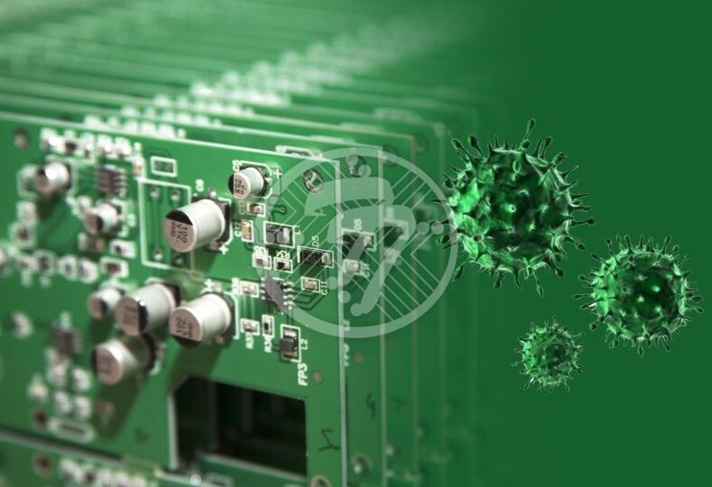
COVID-19 that began in 2019 is a worldwide pandemic that has already taken millions of lives. Apart from being a threat to a person’s health, it is also harmful to the production process of various things. How is it so? Well, COVID-19 became a deadly virus that didn’t have any cures until now. Thus, to make sure people suffer less and live everyday life, the government has imposed various restrictions and laws relating to COVID-19. The world was in a phase of lockdown due to which the supply chains had disrupted. The disruption of the supply change due to COVID-19 led to various problems all around the world. Many businesses shut down due to lockdown and many other restrictions. all this resulted in a significant loss for various production industries. PCB Board Assembly is one of such Products whose development has suffered a lot due to COVID-19.
Even though The Government imposed certain restrictions and lockdown to lessen the impact of COVID-19, still, it led to disruptions to the supply chain of various electronic components.
All of this has been challenging and has affected PCBA assembly service and disrupted its production process. Let’s discuss it in detail now.
Causes of COVID-19 supply chain Disruption
You must be thinking about the causes leading to the supply chain disruption due to COVID-19. There are several reasons behind the turmoil. Some of the main reasons are as follows:
Lack of clarity in Contracts:
In this situation of a global pandemic, people have been suffering losses a lot. All such losses include supply chain disruption. One of the causes of such a situation is a lack of clarity in contracts between Buyers and suppliers. They haven’t come up with a deal including the COVID-19 condition, thus leading to specific problems. Also, such agreements did not include the time of recovery and some processes.
Lack of inventory:
Another reason leading to the disruption in the supply chain of PCBA is the lack of inventory. Even if COVID-19 reduced the manufacturing process, people could still produce PCBA through the existing stockpiles. However, there was a limited inventory of components required for the PCBA Assembly.
Closing down of factories:
closing down of factories also led to PCBA services supply chain disruption. Closing down a factory leads to the end of production as well. And if the components of PCBA are not manufactured, how can its production take place?
Restrictions on import and export:
Many PCBA production industries Depend upon the import and export of various components and parts of PCB for its production. It was going reasonably pre-COVID-19 period. However, certain restrictions have been imposed upon import and export services. Due to this, The PCB production that depended on import and export have been suffering losses.
Impact of COVID-19 supply chain disruption on PCB Board Assembly
Now that you know why the supply chain is being disrupted let’s get to its impacts. Supply Chain disruption Has affected the PCBA Production industry in various ways. Let’s discuss some of its significant effects on PCB Board Assembly below:
Less production:
COVID-19 supply chain disruption has resulted in less production. If there are no parts or components required to make PCBA, how is its production possible? PCBA Services have been reduced since the global pandemic COVID-19 has taken place.
Economic instability:
COVID-19 has resulted in tremendous economic instability as well. Due to such unrest from a financial perspective, production companies didn’t have any luck. At the initial stages of COVID-19, the USA suffered the most, even in economic terms. The PCB Board Assembly in the USA has been having loads of difficulties regarding its production.
Delay in shipments:
Another impact of supply chain disruption on PCB Board Assembly is that there have been several delays in shipments. Some delays were due to production issues as well. Supply chain disruption leads to slow production, which means the more time it takes for production, the more for shipment.
A decline in sales:
There have been numerous reports of a decline in PCBA services sales due to the supply chain disruption caused by COVID-19. PCB Board Assembly has been likely to face a sales slump in 2020.
Ways of protecting PCB Board Assembly from COVID-19 Supply Chain disruption
You don’t have to stress over the supply chain disruption too much. There are specific ways and practices that you can adopt to protect PCBA Services from the supply chain disruption due to COVID-19. Below you can see some of the this you can adopt:
Work cooperatively with your PCB Contract manufacturer:
You cannot question your PCB Contract manufactures Networks and connections in this field. Your PCB Contract manufacture can prove to be of great help to you in such a situation. they have Connections with various distributors and component manufacturers that may come in handy for you.
Work-based on RFT manufacturing of design:
You will be ensuring supply chain continuity if you use the right first-time manufacturing way of designing a PCB Board Assembly. It is the process of manufacturing PCB right on the first try. Due to this, you won’t be required to waste more components or time.
Use alternative components if necessary:
Sometimes, specific components would not be available. Either you can wait for its availability or go for its alternatives. Going for the choice means less time wastage. Thus, you can ask your PCB CM to advise using an alternative component with similar Functions to the one you initially require.
Go for turnkey PCB Assembly and manufacturing:
turnkey PCB manufacturing can be of great use for you during this pandemic situation. You will be saved from Various hectic tasks related to the PCBA Assembly service. You can get help from your PCB Contract manufacturer to optimize all PCB production stages, Including component procurement. You can do all this through an integrated turnkey PCB manufacturing process that your Contract manufacture can help you to employ.
Conclusion
Overall, we can say that the global pandemic COVID-19 has resulted in colossal supply chain disruptions, through which PCBA Assembly Has been quite tricky. Several reasons lead to supply chain disruption during global pandemic, COVID-19. The main reason is the restrictions imposed upon the opening of businesses and factories by the government. Less production of components has led to less production of PCBA.
The PCB production industry has been affected in various ways due to supply chain disruption. There has been a considerably lower rate of work and production, resulting in a loss in sales.
However, you are not to worry that much regarding this supply chain disruption. You can adopt specific measures to fight through this period of suffering, which has been mentioned above.
For more information and to find out how we can assist you, email us your queries at [email protected]. Feel free to contact us for PCB Assembly, Printed Circuit Boards Manufacturing and PCB Prototyping needs!


