The Choice of PCB Assembly plays a major role in speeding up or slowing down supply chain


In supply chain management, a single weak link can significantly impact your business. For those in the electronics industry, printed circuit board assembly (PCBA) often becomes that critical link.
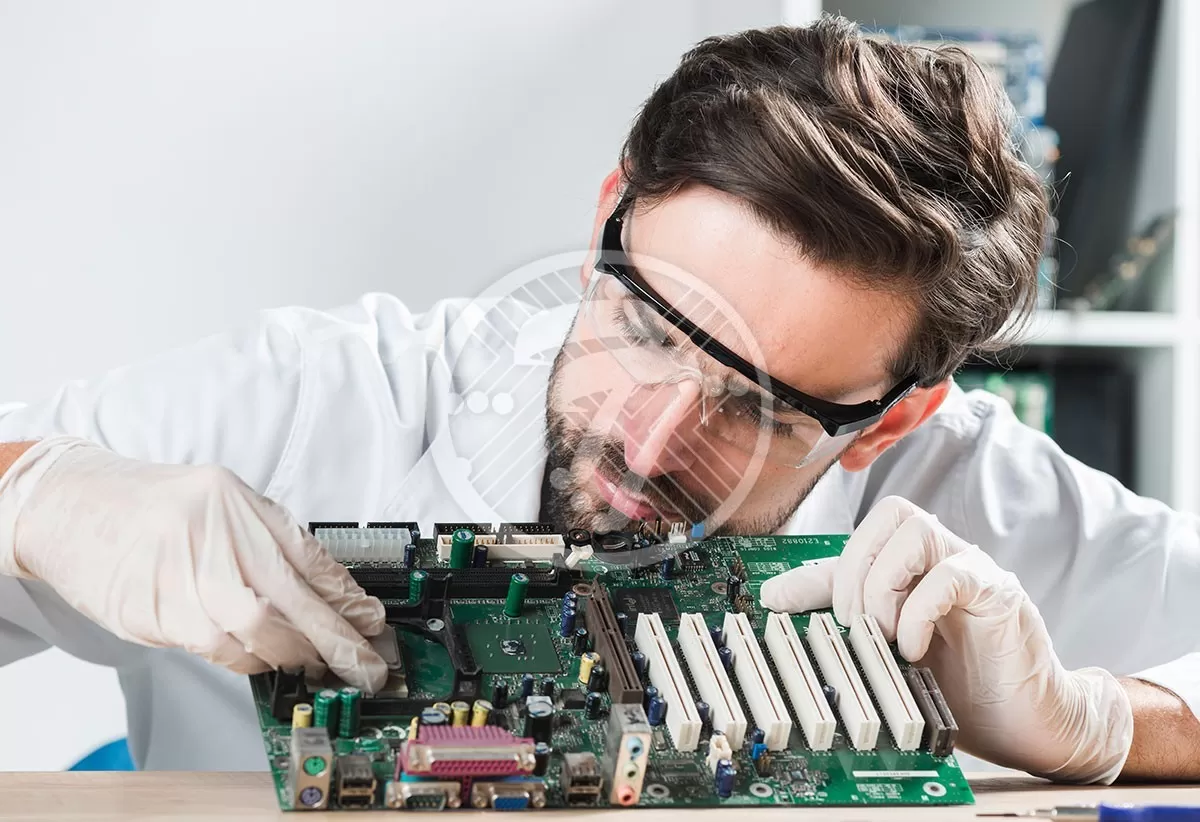
Selecting the right PCBA supplier is crucial. It’s essential to choose a supplier who not only ensures high-quality standards but also leverages their experience to enhance supply chain effectiveness.
One key benefit of choosing the right PCBA supplier is their ability to audit not just PCB layouts but also prototypes. This means they can align engineering schematics with speed considerations from the start, helping you bring products to market faster.
To ensure that your supply chain operates efficiently, consider these strategies. By integrating printed circuit board manufacturing into your supply chain, you can address potential bottlenecks and speed up your production process.
#1 Have proper communication channels
When you are on a tight deadline, there is little scope for a communication breakdown. Ensure therefore that communication with the PCBA is clear and responses are not delayed. It is best to avoid assumptions as far as possible and put everything in clearly understandable terms, well in advance as far as possible.
In fact good partnering practices with your PCB supplier include:
- Routine conference calls between your team and that of the PCB supplier
- Quarterly Reviews that are designed to review the performance metrics and any business updates. Ideally this can be a two way process with updates being shared from both sides related to any business growth, new products and more. Essentially any information that impacts the production process as well as the business relationship needs to be shared.
- Supplier score cards with objective and subjective metrics is yet another process that should be maintained. Things such as on-time delivery, defect rates as well as communication issues and more should be flagged off from time to time so that everyone is aware of issues, if any.
- You also need to ensure that the supplier has a quality improvement program in place with periodic reviews.
The above best practices will ensure that the process is kept under check and also that the equation with the PCBA is that of partnership and not just of a vendor.
#2 Ensure that your documentation is complete
Ensure that you have worked through your documentation well in advance and that the documentation includes the following:
- Bill of Materials – Do remember to go by the format that the supplier prefers
- Gerber Files
- XY data file
- Stencil Files
- Special assembly instructions
If there are any sub-assemblies that need to be manufactured in advance, it is also imperative that you have a bill of materials for each sub assembly and estimate the lead time for the parts. It is also important to verify their compatibility with the finished product
Try and avoid any last minute changes to ensure that everything is in order well in advance.
#3 Identify parts which have long lead-time
Ever so often electronic components have long lead times, often running into months. Identifying these components early can help the PCBA look for either alternate parts or source suppliers who have shorter lead times. In turn this can help cut lead times significantly as also impact costs.
#4 Forecasting demand
Keeping the PCBA posted on the demand forecasts instead of waiting to inform them of out of stock products at the last minute can also go a long way in keeping cost in check. It is commonly known that express shipping can come at a far higher cost and can derail the overall costing. Keeping the supplier posted on demand forecasts, on the other hand can offer the lead time to procure supplies at efficient rates.
#5 End to end partnership
Look for a PCBA who can provide end-to-end solutions and can assist you right from the conceptualization to the production phase. This will streamline the entire process and will cut down time.
The above steps when followed can ensure that the PCB Assembly process and the PCB Assembly provider does not become the weak link in your supply chain and is instead recognized as a critical part of the entire operation.