Top Causes of Warpage in PCB Assembly Process & Their Prevention Measures!

By | Date posted: | Last updated: April 8, 2022
Warpage in PCB

With the miniaturization of electronic devices, the use of thin PCB circuit boards and small components is in vogue. However, the use of thin multi-layer PCBs with small SMT components also brings some issues in its wake. Typically, such PCBs suffer from warpage in the PCB assembly process that impacts among other things, its yield. Besides, excessive warpage also leads to the quality of the paste printing being affected. Warpage also affects the formation of solder joints during the reflow soldering process.

Before we get to the solutions that can help control warpage, let us have a quick understanding of what warpage really is.

What is PCB Assembly Warpage?

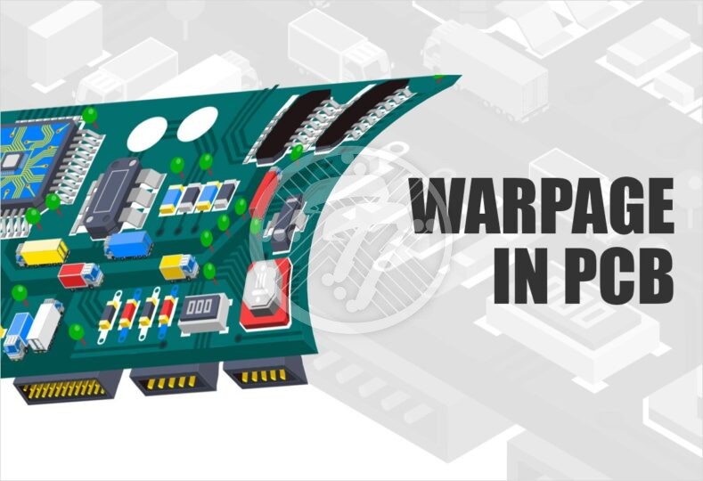
Typically, all parts of the Printed Circuit Board should be in contact with the surface. However, sometimes on account of various stresses this does not happen. What we have is a condition where some parts of the PCB bend upwards and some downwards resulting in positive and negative curvature. Sometimes the bend may be along the axes of the board or along the diagonals. The board can sometimes also develop a twist. All these are examples of PCB warpage.

Causes of Warpage in PCB Assembly

  • Built in stress on the copper film causes the boards to warp. This is possible even at room temperature without any thermal process.
  • During processes that involve temperature changes, such as reflow, warpage is caused on account of the difference between the coefficient of thermal expansion between the copper layer and the substrate.
  • When individually etched copper clap boards are stacked together, the difference in copper density of each layer causes differing amounts of stress on each layer leading to warpage.
  • PCBs are often placed in a panel so as to improve PCB assembly efficiency. Panelization, in turn, uses rails and outriggers. Post assembly, the outrigger is removed and the PCBs are separated by de-paneling them. The difference in copper density in the board area as opposed to the outrigger area further causes warpage.

Issues Caused due to Warpage in PCB Assembly

  • In case of a warped PCB, some parts of the PCB become closer to the stencil and some parts are further away. In turn, this causes solder paste deposits on the closer part of the PCB to have a lower height. The deposits on the parts with a larger gap have a greater height. With this non-uniform solder paste deposit a number of issues are seen. These include:
    • Stretched joints
    • Open joints
    • Solder bridges
    • Head & Pillow joints
  • When the temperature increases, such as in the process of reflow, its warpage increases. In turn, it can affect soldering under close-pitch ICs.

Ways to Prevent Warpage in PCB Assembly

IPC-A-610E standard specifies maximum warpage for incoming PCBs at room temperatures. As per IPC-TM-650, the maximum bow and twist for an SMT PCB must not exceed 0.75%.

To control warpage in PCB assembly, the following steps are recommended:

  • Copper Balancing – At the design stage itself, due care must be taken to balance copper across all layers. This helps in minimizing the mismatch in terms of the co-efficient of thermal expansion both at room temperatures as also when the temperature increases.
  • Balancing substrates across PCB layers – In a multi layered PCB due attention must be paid to use substrates with different CTEs. It is recommended that substrate of the same thickness and material be used in the top as well as bottom layers.
  • Balancing copper density – During panelization, the difference in copper density in the rails and outrigger areas of the panel needs to be minimized.
  • Pallet Design – It is recommended that the temperature difference between the PCB & pallet is minimized. Also the clearance between the PCB edge and the pallet edge needs to be kept minimal. It is also prudent to use low spring force to hold down the perimeter and corners of the PCB. Providing adequate support to the pallet so that the PCB does not sag at high temperature, is also recommended.
  • Pre-Treatment – It works well to bake the PCB above its Tg. This helps soften the laminates as also relieve the stress in different layers. Warpage is thereby, minimized.

To sum up

It is important to go with a PCB contract manufacturer who has a thorough understanding of the various issues that can cause PCB warpage. The above tips can go a long way in ensuring that warpage is kept at acceptable levels.

Technotronix is one of the leading PCB manufacturers in the USA. We have over 4 decades of experience in providing innovative PCB manufacturing services using modern technologies & the latest machinery. We are adhering to strict high-quality standards and compliant with the RoHS (Restrictions of Hazardous Substance) directives. We can fulfil the varied needs of our customers from the simple board to the most complex board for PCB prototype to production.

The Troubleshooting Guide for Wire Harness and Cable Assembly

By | Date posted: | Last updated: January 18, 2023
wire-harness-and-cable-assembly

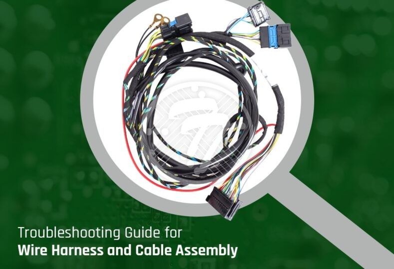
While the term cable assembly and wire harness are often used interchangeably, these are two distinct products that have different uses.

A wire harness typically consists of multiple wires within an exterior sheath. The exterior sheath is made up of thermoplastic or thermoset and does not offer too much protection from friction or temperature fluctuation. Wire harnesses, therefore, do not find extensive application in harsh and demanding environments. Cable assemblies, on the other hand, also have multiple wires covered by an external sheath, however the sheath is made up of heavy-duty material that can withstand environmental pressures. Explore the top difference between cable assembly and wire harness.

Below are some of the problems faced in cable assemblies and wire harnesses; and effective troubleshooting methods for them:

Common Problems faced with Wire Harnesses Assemblies:

  • Not making the right choice of cable – Very often the underperformance or failure of the cable assembly is on account of their inappropriate selection given the environment they must function in. For instance, if the cable isn’t durable enough to withstand force, they could break. In such cases, a pull test is required to figure out its strength.
  • Improper Installation – Incorrect installation of cable assembly can impact their performance. Whether it is a sloppy soldering job or if the die is set incorrectly, it is bound to show deterioration.
  • Testing not done correctly – Post assembly of the cable component, if the testing isn’t done correctly, it can lead to issues that can turn out to be costly in the long run.

Common Problems faced with Wire Harnesses:

  • Improper Wire Preparation – Wire Preparation involves stages such as the right selection of wire, cutting it correctly. Any of this not done correctly can lead to incorrectly prepared components.
  • Improper layout – The wires need to be arranged properly so that they fit into the harness.
  • Improper labeling – Especially when harnesses are mass produced, improper labeling can lead to a range of issues.
  • Crimping and defects related to soldering – These can lead to issues related to the circuit.
  • Missing Components- This can lead to harness failure. It is imperative, therefore that the assembly documentation is double-checked.
  • Improper wire tying- Both tying the wires too tightly and tying them loosely can come with its own set of problems.

Intermittent Errors in Cable Assemblies and Wire Harnesses:

Common intermittent errors in cable harnesses and wire assemblies manufacturing process include:

  • Opens
  • Shorts
  • Mis wired

These can be on account of a wide range of issues such as:

  • Poor setup
  • Weak contact
  • Pin not seated correctly
  • Damaged Housing
  • Worn or dirty contacts

Despite all possible efforts undertaken to ensure there are no errors in cable assemblies and wire harnesses, inadvertent errors can still creep in. To avoid this, it is important to test the components thoroughly. Some of the common testing mechanisms include:

Mechanical Testing

This ensures that the mechanical properties are tested to see that they meet the requirement of the application. Some of the mechanical properties to be tested include:

  • Elongation
  • Tensile Strength
  • Flexibility
  • Impact resistance
  • Cycles to failure, and more

Environmental Testing

This primarily involves testing to see that the cable assembly or wire harness can withstand environmental conditions such as:

  • Humidity
  • Temperature
  • Vibration, and more

Electrical Testing

The electrical testing largely involves testing for:

  • Open Wires
  • Incorrect Wiring
  • Risk of shorts

Visual Testing

Visual testing involves looking for all components and ascertaining if they are in good condition. Some of the aspects to watch out for, include:

  • The wires and cables, their placement and whether there is any damage.
  • Whether the connectors are proper.
  • Whether the labeling has been done accurately.

Signal Integrity Testing

This involves assessing the signals that the cable assembly or wire harness can carry. You also need to check for crosstalk and signal errors. Also, it is important to see if the use of connectors, filters etc. ensures that signal strength can be maintained.
A judicious use of both the troubleshooting mechanisms as well as robust testing practices will ensure that you do not face performance issues with cable assemblies and wire harnesses.

Being a leading PCB manufacturer from past over 40 years, Technotronix is providing wire harness and cable assembly services in USA. It ranges from simple to every complex cable and wire harness assembly with quick turnaround time. Technotronix is specialized in layout and assembling of custom and complex cable and wire harness assemblies to address the needs of customers. We cater to the wide spread needs of our broad customer base of varied industries like aerospace, defense, telecommunication, medical etc.

For more information, get a quick wire harness and cable assembly quote or contact us via email at [email protected] or call us on 714/630-9200.

In-Circuit Test (ICT) vs. Flying Probe Test: Which one is best for your Electronic Board Assembly!

By | Date posted: | Last updated: February 14, 2022
in-circuit-test-vs-flying-probe

When it comes to making a decision about the best testing method for your PCB, they are a number of factors to consider. Some of these include:

  • Costs- both up front as well as per unit
  • Coverage
  • The lead time involved
  • Customization
  • Whether or not it suits the complexity of your design

While both the tests are equally equipped to discover defects such as opens, shots, resistance, capacitance, and component orientation, their differences lie in the following areas:

  • Development Time involved
  • Coverage
  • Costs per unit
  • Custom tooling
  • Engineering charges

Let us take a detailed look at In-circuit vs Flying Probe testing on these criteria as also determine which is most suited for your electronic board assembly.

In-Circuit Testing

The way In-circuit testing or ICT, as it is popularly known works, is that it uses a bed of nails to access the circuit nodes and then check the performance of each component. It can also test the functionality of digital circuits, however, the cost involved there is substantial.

Typically, the strength of ICT lies where you need to test products that are high volume. It is also useful in testing well-developed products. However, since ICT requires that a custom fixture be created, the costs involved as well as the lead times are high. However, the advantage of ICT lies in the fact that once you have the custom tool ready, the per unit costs are low.

If we were to summarize the Pros & Cons of ICT, they would look as under:

Pros

  • It lends itself to quick tests per PCB unit.
  • The per unit costs are low.
  • It can test individual components.
  • It works well when you need to test logic functionality.
  • It can be used to test LED components.
  • You can use it to test BTC component soldering by way of a pressure test.

Cons

  • The lead time involved in development tends to be long, which can be an issue in today’s times where a quick go-to-market is a source of competitive advantage.
  • The high up-front cost can be detrimental in its usage.
  • It requires the use of programming tools.
  • You cannot use it to test either non-electrical components or to test connectors.
  • While it can be used to test individual components, it does not lend itself to testing components working together.

Flying Probe Testing

FPT (Flying Probe Testing) uses both movable and fixed probes to test the top and bottom of your PCB. It uses high-precision needles, which are programmed to undertake electrical and PCB functional tests.

As a thumb rule, Flying Probe Testing works well for low-volume orders. It is also suitable for products that are in the initial stages of development. Since it does not require custom tooling, the costs of FPT, work in an inverse manner as compared to ICT. So, FPT has higher per unit costs as opposed to high up-front costs of ICT.

Let us look at the Pros and Cons of using FPT:

Pros

  • It does not require any custom tooling saving upfront costs and time.
  • You do not have to waste precious time in programming.
  • It is best used to test components individually.
  • It can be used to test LEDs.
  • It has low upfront costs.

Cons

  • The per unit costs are high.
  • It cannot test connectors as well as non-active components.
  • While it can test components individually, it is not suited to test components working together.

Which works better, ICT (In-Circuit Test) or FPT (Flying Probe Test)?

There is no one-size-fits-all when it comes to the choice of ICT or FPT. The choice truly depends upon your individual project requirements. You need to look at factors such as whether you want to go in for low volume or high-volume testing, what kind of lead times you have available, your overall budget as well as the complexity of your PCB design in coming to a well-thought-out decision.

It is important to discuss each of the options with your electronic contract manufacturer. It is imperative that the PCB contract manufacturer you are working with has a complete understanding of each test system and can advise you on which one will work best for your specific needs.

Technotronix is one of the leading printed circuit board manufacturers based in the USA. We have over 4 decades of experience in providing innovative PCB manufacturing services using modern technologies and the latest machinery. We are adhering to strict high-quality standards and compliant with the RoHS (Restrictions of Hazardous Substance). To know more, please contact us.

Manual Vs. Automated Assembly – Which one is right for you?

By | Date posted: | Last updated: February 15, 2023
Manual vs. Automated Assembly

When it comes to PCB assembly process, the importance of automated assembly is well known. After all it offers the much-needed speed and consistency that your manufacturing needs. Does this mean that manual assembly has no place in today’s milieu? Far from it! Let us look at the use cases for both, to help you decide which one is right for your manufacturing process of PCBA.

Importance of Automated Assembly

Clearly its importance comes from the fact that it offers speed which makes go-to-market, that much easier. It can therefore be a big source of competitive advantage. The other major advantages that it offers include:

Low Cost

Professional PCB Assemblers use the circuit board assembly program before getting into actual production. In turn, this reduces both errors as well as the possibility of delay. It is also possible to correct any design errors in the interim. Overall, what this leads to is significantly lower costs.

Reduced chances of errors

The printed circuit board assembly process requires great attention to detail. This is especially true on account of the circuit boards getting increasingly smaller. As opposed to manual assembly, an automated assembly significantly reduces the chances of errors. What this means is that you get a reliable product and do not have to contend with costly errors when you are ready to send out the final product.

Consistent quality

The big advantage that automated assembly offers is that you can be assured of consistent quality. This clearly isn’t the case with manual assembly as there is human intervention involved.

Miniaturization

With Miniaturization, it is often not possible to assemble the components manually, necessitating automated assembly processes.

In addition to these general advantages of automated assembly, PCB Automated Assemblies, in particular benefit from the following facts:

  • Large components need automated solder reflow since it is difficult to manually soldering pins particularly that are hidden underneath.
  • QFPs are sensitive to co-planarity and are hard to manually solder.
  • Small components such as resistors and capacitors are hard to manually solder.
  • For boards where components are densely placed, consistency in manual soldering is always an issue.

Some of the automated systems used by Contract Manufacturers include:

  • Marking & labeling systems for component and PCBA identification.
  • Pick-and-place machines for placing parts on the board.
  • Soldering systems for placed parts
  • Automatic routing machines
  • In addition to the assembly systems, there are also automated testing systems that include:
    • Optical Inspection Systems
    • In-circuit test systems
    • Flying probe test systems
    • Functional testing systems

Importance of Manual Assembly

The advantages of the Manual Assembly system from:

  • When it comes to low-volume PCB assembly; manual assembly is both faster as well as economical. Particularly through-hole components work well with manual assembly when it comes to low volume runs.
  • Prototypes also benefit from manual assembly since you are looking at low volume runs as also unusual component placements.
  • Some components cannot be well inspected by way of automated optical inspection and need manual intervention to verify placements as well as to check for any soldering issues.
  • When it comes to surface mount connectors, once again manual inspection may be needed.
  • At times during the process of reflow, you could have small components floating up that require manual cleanups.
  • Manual processes also work well when you are looking for repairs and rework for existing PCBs.

Therefore, each of the two methods offers its own set of advantages. There cannot be a one-size-fits all solution. So, while you will use automated assembly for its speed, consistency, lower costs, and more, there are enough and more occasions where manual intervention will be required. What is required is that you partner with an electronics contract manufacturer who has the requisite automated assembly equipment as also a skilled team; so that you can use the right method given your bespoke requirements. Next-generation equipment as also experienced manpower that is equipped with industry best practices can make a lot of difference when it comes to churning high-quality PCBs.

Technotronix is one of the leading PCB manufacturers in the USA. We have over 4 decades of experience in providing innovative PCB assembly & manufacturing services using modern technologies & the latest machinery. We are adhering to strict high-quality standards and compliant with the RoHS (Restrictions of Hazardous Substance) directives. We can fulfil the varied needs of our customers from the simple board to the most complex board for PCB prototype to production.

Get a quick PCB assembly quote!