Top 10 Best PCB routing practices!


Routing a circuit board comes with its own set of challenges. Especially when we are dealing with miniaturized boards and high-speed signals, the challenges get further enhanced. If you are looking for industry best practices when it comes to PCB routing for high-speed designs, here are 10 handy tips:
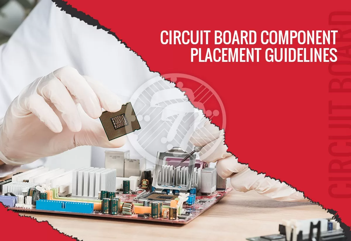
PCB routing practices
1. Have a common ground plane below signal traces
It is recommended that high-speed signals be routed over a solid ground plane. Using at least a 4-layer PCB is also beneficial, as then one of the layers can be used as a ground plane. While sometimes a double-sided PCB may be required to be used, the fact remains that when you need to route tracks on both sides, you do not get a solid ground plane. In such cases, at least under critical sections, a ground plane should be attempted. Broadly, full single ground planes offer better results than split grounds.
2. Ensure vias are placed in a grid
It is imperative that blind and buried vias are positioned accurately as otherwise it can result in hotspots. As a thumb rule, vias should be placed 15 mils apart from each other.
3. Ensure that trace bends are kept at the minimum
When routing high-speed signals, bends need to be kept at a minimum. In the situation where you need to keep the bends, 135 degrees is a far better option than 90 degrees. This will ensure that PCB etching is smooth.
4. Maintain a minimum distance between traces
This will ensure that there is minimal crosstalk as among other things, crosstalk is a factor of the distance between traces. Due emphasis therefore needs to be placed on the fact that the traces aren’t closer than desirable.
5. Daisy Chain Routing
If long stub traces are used, there is often a compliance issue with EMC standards. Besides this, signal integrity can be negatively affected. In case it is important to use pull-up or pull-down resistors, it is recommended to use daisy chain routing.
6. Avoid placing components between differential pairs
It is important to have differential pairs parallel to each other. Also, symmetrical routing should be followed for differential pairs. Placing of vias or components between the differential pairs is a strict no-no as it could lead to issues with impedance. In case you need to include serial coupling capacitors, ensure that they are placed symmetrically. Another aspect to keep into account is that both traces should be routed on the same layer.
7. Avoid a split plane while routing signals
The use of a split plane needs to be avoided as such a signal path can lead to EMI issues. If you have a situation where the plane is split between a sink & source, the signal trace is best routed around it. Similarly, if a signal needs to be routed over two different reference planes, stitching capacitors should be used. The position of the capacitor is crucial as the distance between the forward & return path needs to be kept small.
8. Ensure that the analog & digital ground planes are kept separate
This will make it easy to determine which components should be connected to the digital ground & which one to the analog ground. For mixed signal circuits, the analog & digital ground needs to be connected at a point. Zero-Ohm resistors between analog & digital sections are recommended. Also, if the mixed signal design has split planes, you need to take care to see that the digital signal is not routed over an analog ground plane & vice versa.
9. Create a virtual separation in the layout with respect to analog & digital ground
This virtual separation needs to be kept in mind during the routing process. Due care needs to be maintained to see that the analog or digital trace does not crossover to the other side.
10. Keep the width of the component as close as possible to the track width
By doing this, the impedance matching issues between the track & the component pad can be addressed.
With the above tips, you can ensure that your design is robust & that there are no manufacturability issues, causing you loss of precious time when the industrial printed circuit board comes to the manufacturing stage.
Technotronix provides a one-stop solution for electronics manufacturing services with specialized support, reliable testing, and multi-functional features. In case if you have any questions, please feel free to contact us via email at [email protected] or call us at 714/630-9200.