The bill of materials in PCB design: The best practices for long-term production!

By | Date posted: | Last updated: September 4, 2024
Bill of Materials PCB

Designing a new circuit board needs meticulous planning for sure. When you are designing for long term production you need to have specific and detailed strategies in place so that you can avoid any component shortages. Here are some specific supply chain problems that have been staring at the industry particularly in today’s times:

Short supply

With the global pandemic, component short supplies have been a reality. With inventories at OEMs dropping, designers are forced to look for alternative parts. The supply chain shortage is also impacted by the global shipping problems. Vendors are unable to reach supplies to customers on account of inaccessibility to the regular shipping channels.

Counterfeit parts

A number of counterfeit parts have also flooded the market. There have been instances of substituting false part numbers whereby general parts are repurposed. There are also instances of old parts being sold as new. It is imperative, therefore, for OEMs to be able to recognize old, counterfeit parts.

In such a scenario Bill of Material (BOM) planning strategies are absolutely important. Let us look at some of the PCB Design BOM planning strategies in detail

PCB design BOM planning strategies:

Check for part availability as well as prices

Before committing to use any parts you certainly need to find out if they are available and their price. It is a possibility that they may have become too expensive. You also need to validate the sources so that you are sure that you do not land up with counterfeit components.

Check for alternative options

In case the parts that you are looking for are unavailable, here are some of the alternatives to consider:

  • Alternative Parts – You need to look for parts that can offer similar functionality. It may be a good idea to also look for combinations of parts that can offer similar functionality. This of course could have a cost implication. However, it will keep your project on track.
  • Redesign – In some cases in order to tackle the issue of the unavailable part, you may need to redesign the circuitry. You also need to look at alternatives where you design the primary component and its alternatives into the board.
  • Forward planning- Above everything, you need to make sure that you time yourself well. Waiting till the end of the design cycle and then beginning to look for parts that you need and finding them to be unavailable, is a sure fire way to disaster. You need to start planning early in a way that you can map the completion of your design schedule with availability of components. There are electronic component specialists that can help with BOM planning.

Having discussed BOM planning strategies, let us also look at some BOM planning resources that can come in handy

BOM Planning Resources

One resource that will stand you in good stead, is of course your contract manufacturer. Ensure that your electronics contract manufacturer has a dedicated engineering as well as procurement team that ensure that you do not fall short by way of unavailability of components. The contract manufacturer will undertake a detailed review of the BOM. They will ensure that the parts mentioned in the BOM work well and are available for use. A strong procurement team will then ensure that the lead times and prices are optimal.

This is not the only way the contract manufacturer can come to your aid. Importantly, a professional contract manufacturer will also review your PCB board design to see that there aren’t any issues that can later affect the manufacturing process. Timely detection of these issues will help prevent costly mistakes. They will also suggest alternate designs that will aid in manufacturability. With their experience and access to industry best practices, you need not reinvent the wheel.

Importantly, if you as a customer work with the contract manufacturer on long-term builds of circuit boards, they will monitor availability of components on a continuous basis. At any time if any part becomes obsolete, the team will have its recommendations ready proactively. This will ensure that your production isn’t impacted and that time to market, which is a big source of competitive advantage in today’s milieu, isn’t impacted.

Technotronix is one of the leading PCB manufacturers based in the USA. We have over 4 decades of experience in providing innovative PCB manufacturing services using modern technologies and the latest machinery. For any kind of PCB manufacturing services, Get a quick quote!

What is a Heat Sink Printed Circuit Board and its importance in the electrical industry?

By | Date posted: | Last updated: May 13, 2022
Heat Sink PCB

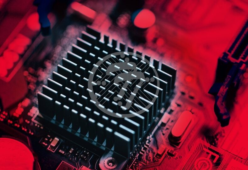
Heat sink technology is of tremendous importance as it allows heat to dissipate and to spread through a circuit. A heat sink PCB is therefore a type of printed circuit board that helps in dissipating high surface temperatures. In fact, heat sink PCBs offer one of the best forms of thermal management. They are ideal for use in applications that generate heat. Most electronics that use heat sink PCBs, therefore, have a longer lifespan.

Why are Heat Sink PCBs important in electronic circuits?

High power devices are known to produce heat. They however have low heat dissipation capability. Some of these devices include:

  • Power transistors
  • LEDs
  • Lasers, and more.

Heat build-up can cause premature failure in the device. Heat sink board, therefore, are the perfect answer.

Benefits of Heat Sink PCBs:

Passive Heat Exchange

Heat sink PCBs can act as passive heat exchangers. With heat dissipated, it leads to improved performance of the device and prevention of device failure.

Maintains Thermal Stability

What heat sinks in PCBs help to do, therefore, is to maintain the thermal stability of the device. In high-performance applications, therefore, their importance cannot be overstated. Additionally, other than heat dissipation they also provide heat during low temperatures. The generation of thermal energy, in turn, allows for the smooth functioning of the circuit.

Spreads heat

In some applications, heat sinks help to spread heat. For example, in case of graphic processors and CPUs of computers, they come in extremely handy to spread heat.

Prevents system failure

In the absence of a heat sink, there is high risk of failure of components. Typically, in mission critical operations, this can be a huge problem.

Types of Heat Sink:

The various types of heat sink are as below:

Active heat sink

Such heat sinks are powered by water pumps and fans, for example, which increase the rate of heat transfer. In some systems these coolers run off the internal power supply. The moving parts of this heat sink do not make it ideal for long-term applications of PCB industrial solutions.

Passive heat sink

Unlike an active heat sink, a passive heat sink does not feature any additional products or processes. In such cases the heat dissipation takes place through the process of convection. Such heat sinks are bigger than active heat sinks.

Types of heat sink based on material:

Aluminum heat sink

Aluminum heat sinks are a popular choice on account of the thermal conductivity of aluminum. In such heat sinks, the heat escapes through thin metal fins. Additionally, the fact, that they aren’t too expensive, adds to their popularity.

Copper heat sink

Copper is known to be a good thermal conductor and has great heat transfer capabilities. However, heat sink PCBs made of copper are more expensive.

Finned heat sink

This type of heat sink is designed in a manner that a large number of thin plates extend outwards from the central block. They offer a high surface area and hence effectively transfer heat away from the components. Typically, such heat sinks use either die-cast or forged models.

Pinned heat sink

This type of heat sink features rods or pins that extend outwards or upwards. While they work well in terms of the overall surface that they offer, they aren’t particularly known for their superior performance.

Heat sink types based on manufacturing techniques

Based on the PCB manufacturing process or techniques, heat sinks can be classified as under:

Stamped heat sink

This heat sink uses stamped metals. Such metals can form a certain shape. Such heat sinks work well for low-power applications.

Bonded heat sink

This kind of heat sink works well for large applications. They are formed by combining separate fins to the base of the heat sink, by either brazing or thermal epoxy.

Skived heat sink

These use fine blocks of metal for manufacturing heat sinks.

Swaged heat sink

These use a cold working forging process for its manufacturing.

Forged heat sink

Such heat sinks make use of compressive forces. This is particularly used in aluminum and copper heat sinks.

Machining heat sink

The machining process is used for manufacturing such heat sinks. However, since it leads to considerable metal wastage, this method is expensive.

To sum up, the characteristics of a good PCB heat sink include:

  • It should have a large surface area.
  • The heat dissipation needs to correlate with the temperature difference between the device and the ambient temperature.
  • Its flat surface should be in contact with the heat source.
  • Its design should allow for free flow of air through the fins.

We are one of the leading PCB manufacturers in the USA. we are fully equipped to handle your PCB manufacturing requirements. We take an extra step to reach out to your exact PCB manufacturing requirements, high-quality standards, and a strong customer support service to provide quick turnarounds and on-time delivery to our customers.

In case if you have any questions, please feel free to contact us via email at [email protected] or call us on 714/630-9200.

All you need to know about Blind and Buried Vias PCB!

By | Date posted: | Last updated: May 6, 2022
Blind and Buried Vias PCB

When it comes to high density PCBs where you cannot fit all your connections on one layer, vias are extremely useful.

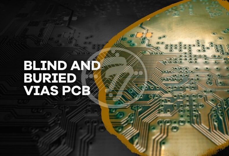
Simply put, vias are barrel shaped vertical conductive holes that help make connections between multiple layers of a PCB.

Blind and buried vias

The two vias are popular when you need to make connections between the multiple layers of a printed circuit board that are blind and buried vias.

To put it succinctly, a blind via connects the outermost layer of the board to one or more inner layers, but does not go through the whole PCB. Blind vias free up space and works well for fine pitch BGA components. They also help reduce signal stubs through the drilling process as the via terminates at the last connected layer.

A buried via, on the other hand connects two or more inner layers but doesn’t penetrate through to the outer layer. As their name suggests, they are hidden beneath the layers and free up surface space without impacting the traces or surface components on the top or bottom layers.

Both blind and buried vias are of tremendous use in High density interconnect PCBs. Such PCBs offer multiple advantages including but not limited to:

  • High layer density
  • Better power delivery
  • Ability to use smaller pitch devices

Types of blind vias

There are broadly four types of blind vias

  • Photo defined blind vias.
  • Sequential lamination blind vias.
  • Controlled depth blind vias.
  • Laser drilled blind vias.

Photo Defined Blind Via

This is created by laminating a sheet of photosensitive resin to a core. The layer of photosensitive material is covered with a pattern that covers the areas where the holes are to be created. It is then exposed to light that causes the material on the PCB to harden. After this, the PCB is immersed in an etching solution. Post the etching process the copper is plated in the hole and on the outer surface. These vias are typically used to create BGA packages.

Sequential Lamination Blind Via

This is created by processing a thin piece of laminate. The laminate is drilled, plated and etched. The other side is left as a solid sheet of copper. The subassembly is then laminated. The combined lamination is processed to create the outer layers of a multilayer PCB. This process needs some extra steps, hence the price of this kind of via is high. Additionally, there is also yield loss that comes with handling thin laminates.

Controlled Depth Drilled Blind Vias

These are created like through-hole vias. The drill penetrates only someway through the PCB. Care is taken to see that no features below the drilled hole come in contact with the drilled hole. Copper is hen plated in the drilled hole and the through-hole vias. These vias are least expensive. However they come with a limitation that the holes must be large enough for the mechanical drills to create them and the area below them must be kept clear of circuits.

Laser Drilled Blind Vias

These are created once all the layers in the PCB are laminated and before the outer layer is plated and etched. With the use of either CO₂ laser or Eximer laser the copper on the outer layer is ablated.

The CO₂ laser is extremely powerful and can quickly drill the holes. However, with this laser the drilling step has to preceded by an etching step. The eximer laser can drill through both the copper balance in PCB and the underlying dielectric material to form a blind via.

The Advantages of Blind Vias

Blind vias help to reduce parasitic capacitance. This is done by shortening the length of the vias and by reducing their diameters. Blind vias are therefore a great way to connect signal lines operating above 4.8 Gb/s.

Some of the limitations of blind vias include:

  • A blind via is a blind hole in the PCB. In order to ensure that the plating is done correctly, the diameter of the hole should be equal to its depth. This requires an aspect ratio of 1:1 or less. Some fabricators require a diameter that is 1.5 times the depth.
  • With a blind via the drilling needs to stop at the intended layer. With a laser drill, while the drill needs to go through copper on layer 1 in should not drill the copper connecting pad that is in layer 2. This requires careful calibration.
  • Another issue is to do with soldering a component to a pad into which the blind via is placed. When solder paste is applied to the pads, the air in the blind via is trapped under the hole that cannot weaken the joint.

Aspects to keep in mind in making vias

Vias can be made before or after multilayer lamination. One or more cores are drilled and through holes are plated. The stack is then built and pressed.

In creating blind vias, it is important to be aware of the drill depth. If the hole is too deep it can impact the integrity of the signal and if the hole is too shallow the connection wouldn’t be proper.

It is also important to plug the vias with either metal or thermal/electrical epoxy and plate it with copper. In the absence of this, bubbles can move upwards and impact the solder joint.

The other aspect to keep in mind is that the vias must cut through an even number of copper layers. Also, if the via is completely enclosed within the terminal point it can lead to a significant increase in costs.

While discussing Blind & Buried Vias it is also important to understand what stacked & microvias are:

A stacked via further helps in improving the size & density considerations of the PCB. It therefore greatly aids miniaturization and high-signal transmission speed.

If you have blind vias with an aspect ratio of greater than 1:1 or if your drilling needs span multiple layers, a stacked via is needed. These are laminated blind or buried vias. Not only do stacked vias save space and help in high-density, they also offer greater flexibility when it comes to the inner connections along with better routing capacity and less parasitic capacitance.

A microvia is a small via that offers more routing space on the board and lower parasitic capacitance. However, such Vias requires more drilling time.

To sum up

The main benefits that blind and buried vias offer, include:

  • You can meet the density requirements and constraints for lines and pads on your design without increasing the overall layer count or the size of your board.
  • They help in saving space and meeting extremely tight design tolerances.
  • They help designers manage the hole-to-pad ratio and restrict chances of breakout.

The issue with blind and buried vias include:

  • They increase the cost of the board. This is because the board is complex and many manufacturing steps are added. Also testing and precision checks need to be added. Between the two, however, buried vias offer a lower cost.

It is important to choose the right electronic contract manufacturing partner who has the requisite experience with blind and buried vias.

Technotronix is one of the leading PCB manufacturers based in the USA. We have adopted advanced methods and technologies, which can give you the finest PCB manufacturing services. Our ability to deliver, unparalleled quality as well as customer service, is what makes us stand out. Both on-time delivery and price competitive products are our USP. The most important element of our success, however, has been the relationships we have developed with our customers.

In case if you have any questions, please feel free to contact us via email at [email protected] or call us at 714/630-9200.

Ceramic Multilayer PCB – Top Advantages and Disadvantages!

By | Date posted: | Last updated: April 26, 2022
Ceramic Multilayer PCB

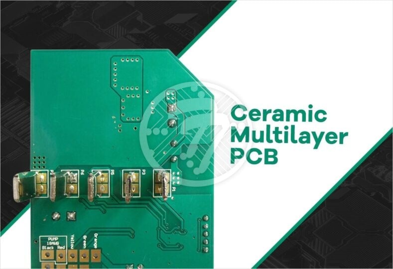
The success of a PCB has a lot to do with the selection of the board material. While FR4 is often used as a default option, the fact remains that there are a number of alternatives that offer better performance and maybe lower costs. Let us look at some of the advantages and disadvantages of a relatively modern technology – ceramic multilayer PCB – that is increasingly gaining ground.

Ceramic Multilayer PCBs

With miniaturization of devices becoming the norm, the PCB industry has been focusing on miniaturization of traditional substrate and laminate PCB materials as well as increased layers. However there have always been challenges around issues such as:

  • Heat dissipation
  • Removal of excesses from the board, and more.

The above has necessitated the search for materials that would work well given the challenges. In many ways ceramic PCBs have been a strong answer. Ceramic materials such as aluminum oxide, aluminum nitride, beryllium oxide and more are seen to perform well on parameters such as:

  • Thermal conductivity
  • Resistance to erosion
  • CTE component compatibility
  • High density trace routing, and more

Advantages of Ceramic Printed Circuit Boards

Before we look at the advantages of ceramic boards in detail, it is important to mention that ceramic isn’t a single material but a class of materials with similar physical and chemical properties.

Thermal Conductivity

A big advantage with ceramic material is its high thermal conductivity. In fact, as compare to ceramic, FR4 has extremely low thermal conductivity. Some figures will put this in perspective:

  • Aluminum Oxide is 20 times as thermally conductive as FR4.
  • Aluminum Nitride and Silicon Carbide are about 100 times as thermally conductive as FR4.
  • Boron Nitride is known to have the highest thermal conductivity.

In case of FR4 PCBs the low thermal conductivity is compensated by using elements such as:

  • Thermal Vias
  • Metal Planes
  • Fans
  • Thermal Landings, and more to direct heat away from the surface layers.

Ceramic boards, on account of their high thermal conductivity, usually do not require these elements as heat can easily be transported to a thermal landing or an active cooling element.

Additionally, the high thermal conductivity ensures that there isn’t any formation of hot spots in the surface as well as the inner circuit layers as heat transport is uniform.

Low Electrical Conductivity

Despite being high on thermal conductivity, the electrical conductivity of ceramics is still low enough for it to be used for PCB substrates. Additionally, it is also possible to adjust the electrical conductivity of ceramic boards through doping.

Do not exert stress on vias

Another advantage of using ceramic boards is that they do not tend to exert a large amount of stress on any vias leading to their fracture. Vias in FR4 boards, particularly are susceptible to fracture during thermal cycling. The risk of fracture is on account of the fact that there are mismatches in the thermal expansion coefficient of copper and FR4. Thermal cycling of the boards, therefore, creates stress along the via barrel and is prone to fractures. In the case of ceramic circuit boards, their thermal expansion coefficients are closer to the values for their conductor structures. This reduces stress during thermal cycling. Also, with the thermal expansion being uniform the stress son any via is significantly reduced.

Mechanical Strength

The big advantage with ceramics is also its mechanical strength. Its ability to withstand high mechanical load as well as strong vibrations and shock can go a long way in their use in harsh operating environments. This is made possible because a ceramic board has a lower Young’s Modulus as opposed to FR4. The ceramic board, therefore, tends to deform much less as opposed to an FR4 board when the same pressure is applied.

Some of the other pros of using ceramic boards include:

  • They resist chemical erosion.
  • Have compatible mechanical intensity.
  • Easy high-density tracing implementation.

This does not, however, mean that ceramic boards come with any disadvantages. The main disadvantages associated with ceramic boards include:

  • They have a higher cost than standard PCBs.
  • They aren’t as widely available.
  • They entail careful handling.

It is important, therefore, to go over the features required by you carefully, in making the right choice of printed circuit boards.

At Technotronix, our highly qualified and experienced multilayer PCB manufacturer ensures that all the layers are correctly registered. Adhering to high-quality multilayer PCB manufacturing practices, we are equipped to handle complex boards with up to 24 layers, which are laminated to insulate them. If you are looking for progressive ceramic multilayer PCBs, you are at the right place.

In case if you have any questions, please feel free to contact us via email at [email protected] or call us on 714/630-9200.