The most common myths & facts about PCB board design!

By | Date posted: | Last updated: March 15, 2022
pcb-board-design

While PCB board design plays an extremely important role, the fact also remains that there are several myths associated with printed circuit board design. Holding on to these misconceptions can lead not just to higher overall production costs but also defective boards. It will be worthwhile to look at some common myths about PCB board design.

Here is a list of the most common misconceptions about PCB board design that need to be debunked:

Design Rules are common for rigid and flexible circuits board

Far from it! There are a number of things that need to be kept in mind depending upon whether you are designing for a rigid or a flexible circuit. Some of the things to be kept in mind include:

  • Flexible circuits need to take into account locational stresses as they need to be folded and bent
  • The design also needs to pay heed to the dimensional stability of the base materials

Component placement does not make a difference

Contrary to popular thinking, circuit performance has a lot to do with careful placement of parts. Placing parts just about anywhere on the board or even grouping similar parts together to save space, does not work. You need to consider a wide variety of factors including but not limited to heat and electrical overload. You also need to consider the height, width and size of components. Every component needs to sit in the right location. Quality PCB assembly also needs to make sure that the PCB doesn’t overheat and isn’t too high on power consumption.

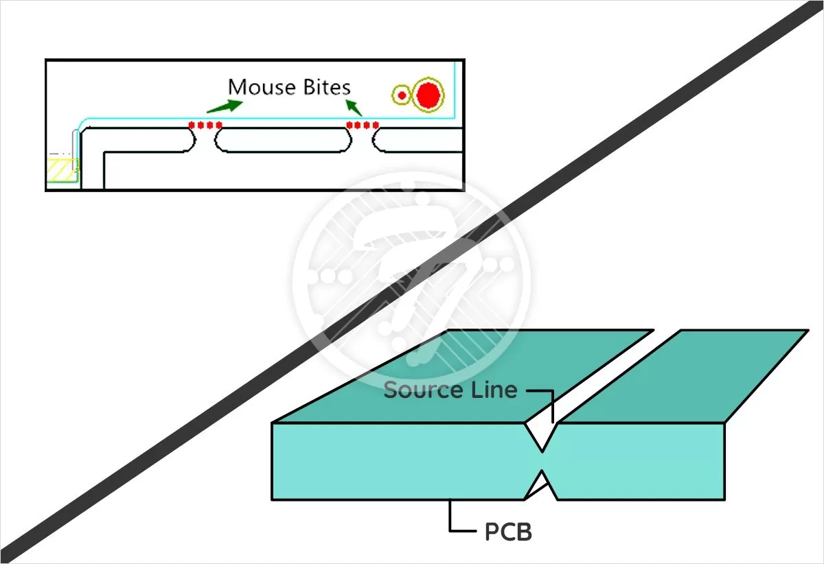
The use of via in pad is not conducive to the circuit board

You certainly need to be careful when using via in pad as plating chemicals can get trapped if you don’t cap or mask it. However, that does not mean that the via in pad should be totally avoided. In fact via in pad have a number of uses, including but not limited to:

  • They work well when you need to place close bypass caps
  • They help in thermal management and grounding
  • They assist in pitch BGA routing

90 degree angles are to be avoided

This is true only when PCBs were etched with acid as the sharp corners would mean acid would collect there. With etching now being done with alkaline, acid traps aren’t an issue any more. 90 degree angles therefore are no longer to be avoided.

Design is all

While it is natural to want your design to be as elegant as possible, the fact remains that other than the design you need to take into account a wide variety of factors. These include:

  • The material available
  • The tools used, and more

While on paper you can have any track width, spacing, annular rig size and more, the final product needs to take into account the real world limitations. A lovely design on paper may not therefore turn out to be effective in the real world. The design, therefore, needs to take into account real world limitations. If this is done correctly, you will not have costly mistakes to contend with at a later date that will cost you time and money and impact your go-to-market.

The design software is inconsequential

The normal tendency is to go with a PCB design software that comes cheap. Nothing wrong there as cost-effectiveness of the software impacts your total project cost. However, choosing the right PCB board design software involves a number of factors other than cost alone. Some of these factors include:

  • Type, quality and quantity of content
  • Availability of community support
  • Integration of supply chain
  • MCAD integration
  • Management of library components, and more

In fact you need to closely evaluate issues like the kind of user interface required, the kind of pricing and more to come to a balanced decision.

With these myths debunked, it is that much easier to pay due attention to aspects that will add to efficiency of design of your PCBs. What this in turn means is the rise of new innovations and a general betterment in the quality of life.

We have over 4 decades of experience in providing innovative high-speed PCB design & manufacturing services. We take an extra step to reach out to your exact PCB manufacturing requirements, high-quality standards, and a strong customer support service to provide quick turnarounds & on-time delivery to our customers. Submit your any custom PCB board design service requirements via PCB design quote form along with BOM (Bill of Material) and Gerber files and we will get back to you soon. Alternatively, you can email your requirements at [email protected] or call us at 714/630-9200.

PCB Mouse Bites vs V-Grooves: What is the difference?

By | Date posted: | Last updated: March 8, 2022
pcb-mouse-bites-vs-v-grooves

Before we look at the difference between PCB Mouse Bites & V-Grooves, it will be worthwhile to begin with looking at what exactly is PCB panelization and what are the various factors to consider in choosing the right technique from amongst the several available.

What is PCB Panelization?

Essentially PCB Panelization allows you to connect smaller circuit boards into a large array. The vendor performing panelization can equally easily depanelize the array. In fact, depanelization is known to increase throughput of PCB.

Factors to Consider for PCB Panelization

The choice of the panelization method depends on a wide variety of factors. Some of these include:

  • Design – Aspects such as clearance between the board’s edge and its components, the presence of edge-hanging components can impact the choice of panelization
  • Components- If the board has sensitive connectors and components, the choice of panelization techniques will be impacted.
  • Materials – The type of PCB material used also determines the panelization technique. For example, some materials are prone to splintering. Similarly, if the boards are very thick you could face issues.
  • Shape – The shape of the printed circuit board also impacts panelization.

PCB Panelization Methods

The broad methods of PCB Panelization include:

  • V-Groove Panelization
  • Tab Routing Panelization
  • Performated Tab Routing or what is known as Mouse Bites

Let us look at PCB Mouse Bites versus V-Groove in some detail:

What is perforated tab routing or mouse bites?

This technique involves drilling small, perforated holes in tabs. It is in their similarity to mouse bites that this technique gets its name. The manufacturer pre-cuts the boards on the array and holds them in place with the perforated tabs.

This method works well where:

  • The components aren’t too heavy
  • It supports edge-hanging component designs which is a source of significant advantage.

The advantages of Perforated tab routing Or Mouse Bites include:

  • They offer a good grip when mounted
  • They work well if you want to use hand separation as a technique of separation.

With perforated tab routing, the areas of concern, however, remain as below:

  • It leaves material on edges. It therefore necessitates sanding. In turn, this not only involves a cost but also consumes time.
  • For holes more than 0.6 inches, a placeholder or knockout might be needed
  • There is a chance of these popping out earlier than needed.

V-Grooves

Also known as V-scoring, v-groove panelization involves separating individual boards housing V-shaped grooves. With this method, the manufacturer can remove 1/3 of the thickness of the board from the top and the bottom. They need to be cut with the help of a machine typically at an angle of 30 or 45 degrees. This method does not lend itself to hand separation as it can put stress on the board as well as its surrounding components.

In this method, the panelization has to have a 0.05 inch clearance from the components to the groove’s center.

V-Groove panelization works well for square and rectangular shaped board. You, however, cannot use it to cut straight lines through the array.

Essentially, this method works well where:

  • There are no overhanging components
  • There are no round corners
  • Where there is a sufficient distance between the component limit and edge of the PCB.

The other advantages of V-Groove include:

  • It is more cost-efficient than mouse bites
  • V-scores are easier to make
  • They offer greater strength

The concerns with depanelizing V-scored PCBs include:

  • It needs a lot of force to break apart and hence requires dexterity to see that components are not harmed during the process
  • In case the copper traces are too close to the score, it can result in splitting.

To Sum Up:

PCB panelization has emerged as an important step when it comes to PCB manufacturing and assembly. By knowing the benefits and constraints of each of the methods outlined above, you can ensure that you do not make any costly mistakes. Also, by knowing the strengths and weaknesses of each technique, redesigns and delays can be avoided, significantly impacting your go-to-market and giving you the much-needed competitive edge.

Technotronix is one of the leading PCB manufacturers based in the USA. We have over 4 decades of experience in providing innovative PCB manufacturing services using modern technologies and the latest machinery. We are adhering to strict high-quality standards and compliant with the RoHS quality management system.

For Any Kind of PCB Manufacturing Service, Get a quick quote!

How does PCB laser drilling work & what are the advantages of using it?

By | Date posted: | Last updated: March 1, 2022
pcb-laser-drilling

When it comes to establishing connections between different layers of a PCB or placement of components, the advantage of laser drilling cannot be overestimated. Laser drilling ensures accuracy even when you need to drill even small holes. It uses concentrated laser energy for PCB laser drilling a hole as opposed to mechanical drilling.

The growing importance of PCB laser drilling

The importance of laser drilling is increasing on account of the fact that the use of HDI technology for PCB designing necessitates the use of microvias. These microvias being small in size require extremely precise and controlled depth drilling. This level of precision is made possible with the use of lasers. The use of mechanical drilling isn’t possible in such cases on account of the following:

  • Mechanical drilling causes drill vibration.
  • It isn’t suitable for drilling holes that are less than 6 mil in diameter.
  • Mechanical drilling does not lend itself to precisely controlled depth drilling.
  • Mechanical drilling is also both expensive as well as a time-consuming process.
  • Mechanical drilling is an expensive, time-consuming process. In a milieu where quick go-to-market is an essential requirement, this does not bode too well.
  • Since mechanical drilling involves hand selection of proper tools, the process can be replete with manual errors. This can lead to costly restarts impacting the overall project cost and timelines.

Laser drilling, on the other hand, can drill holes as small as 2.5 to 3 mil vias on a thin glass reinforcement. Where there isn’t a reinforced dielectric, it is possible to drill 1-mil vias as well.

Advantages of PCB Laser Drilling

If one was to look at the major advantages of laser drilling, therefore, they include:

  • No drilling vibration – Since laser drilling is a non-contact process, it does not lead to any drilling vibration. There is also no damage induced to the material.
  • Accuracy – The big advantage with laser drilling is that it is possible to control the beam intensity, heat output as well as the duration of the laser beam. That it means precision and accuracy in the kind of holes, is a given!
  • High Aspect Ratio – With laser drilling, it is possible to offer a high aspect ratio. A typical microvia is known to have an aspect ratio of 0.75:1.
  • Multi-Tasking – It is also possible to use laser machines for processes such as welding and cutting.

Different Types of laser drilling

laser-drilling-pcb

Laser drilling is possible in several types: important among those being:

Single pulse/Shot laser drilling

This kind of drilling is one where both the source of laser as well as the work material is kept static and where a single shot of laser beam is fired.

Percussion laser drilling

In this method, a series of laser pulses are shot. It works well in creating deeper and smaller holes.

Trepanning

In this process, a laser beam is guided around a predefined locus. It is particularly helpful where the diameter of the required via is larger than the diameter of the laser beam.

Helical laser drilling

In this method, the laser beam follows a helical path while rotating on its own axis.

Although laser drilling comes with a wide variety of advantages as detailed earlier, there are also some considerations that need to be kept in mind when using it.

Consideration for PCB Laser Drilling

Non-homogeneity of the stack-up

It is important to remember that different materials tend to absorb energies at different rates. It is, therefore, important that the PCB stack-up is kept homogenous as far as possible. With PCB materials that have varying optical and thermal properties, the reaction of the laser beams is also different. In turn, this leads to inaccurate drilling.

The thickness of copper

As a thumb rule, the thickness of the target copper layer should be twice the thickness of the top copper layer.

To Sum Up

As long as aspects such as the above are taken care of, laser drilling is indeed the best choice in creating microvias. With the increase of miniaturization as well as high density of wiring and components, the use of laser-drilled microvias is only slated to increase.

Technotronix is one of the leading PCB manufacturers based in the USA. We have adopted advanced methods and technologies, which can give you the finest PCB manufacturing services. We are adhering to strict high-quality standards and compliant with the RoHS (Restrictions of Hazardous Substance) directives. In case you have any questions, please feel free to contact us via email at [email protected] or call us on 714/630-9200.

The Significance of AS9100D Certification in Aerospace PCB Manufacturing!

By | Date posted: | Last updated: February 24, 2022
Aerospace PCB Manufacturing

When it comes to mission critical industries, printed circuit boards have to meet rigorous standards. The boards have to be high on reliability, low on maintenance and also have to perform under difficult environmental conditions.

It is for this reason that the AS9100D certification has been instated as a global aerospace manufacturing standard for the aerospace industry. It covers:

  • Aircraft component and materials manufacturers
  • Aircraft part and assembly designers
  • Quality management organizations and other companies that work with aerospace manufacturers

The certification ensures that certified PCB manufacturers and designers work relentlessly towards delivering highest quality PCBs.

What really is the AS9100D certification?

Released in 2009, this standard incorporates all the requirements of ISO 9001 requirements with additional industry specific requirements for aerospace and defense industries. In fact, most aerospace manufacturers and suppliers require compliance with AS9100 as a condition of doing business with them.

Broadly AS9100D focuses on 5 core processes in the aerospace industry, namely:

  • Quality Management Systems
  • Management Responsibilities
  • Resource Management
  • Product Realization
  • Measures of Improvement

By doing this, it ensures there is uniform compliance.
As far as the certification process for AS9100 goes, it is quite extensive and among other things involves:

  • 2 on-site audits
  • Various internal audits
  • Annual surveillance audits, and more

To obtain this certificate, electronics manufacturers have to follow a stringent list of standards over and above the basic ISO 9001 requirements. Not just that, contract manufacturer has to continue to fulfill the accepted standards year on year for renewals. Some of the standards that need to be fulfilled include:

  • Better configuration management than ISO9001
  • Risk management procedures
  • Industry-critical processes
  • Focus on timely delivery
  • Supplier approval process
  • Prevention of counterfeit components

Essentially, the goal of the certification is to demonstrate that the electronic contract manufacturing partner can offer products that meet statutory guidelines as well as customer requirements.

The AS9100D certification is contingent on the following aspects:

  • Product safety – This of course is the key consideration of the certification. Product safety needs to be demonstrated through the entire cycle of the PCB as also high-temperature applications.
  • Risk Based Thinking – Risk of course needs to be factored into all products including PCB boards. With rules around risk management becoming more stringent, proactive steps need to be taken to remain compliant.
  • Counterfeit Parts Prevention – The latest certification includes a whole lot of clauses that ensure that the use of fraudulent products is identified and stopped.
  • Human Factors – Under this certification, human failures are seen as a part of the failure of the system and it therefore offers an opportunity to improve the overall process.

Advantages of AS9100D certification in aerospace PCB manufacturing

With an AS9100D certification, you can rest assured that the contract manufacturer is committed to providing high-quality aerospace electronics PCB assembly & design. Some of the advantages offered include:

  • Customer Satisfaction – Whether you are looking at prototypes or full production runs, with an AS9100D certification you can be assured of complete satisfaction whether it is to do with PCN quality and its adherence to stringent quality standards or that the boards will be delivered on time.
  • Optimal Costs – With the AS9100D certification offering continuous improvement to the manufacturing operations, what it also brings is cost-effective price points.
  • Turnaround times – The processes so honed, offer quick turnaround times that make go-to-market that much easier.

Keeping up with AS9100 certification

Once electronics manufacturing companies earn the certification, they need to go through regular renewals. This ensures that they are complying with revisions if any. Recertification audits ensure that compliance is fully followed. While the recertification audit verifies compliance with all clauses of the standards, surveillance audits only review a sample of the clauses.

To sum up

With AS9100D Certification, you can rest assured that your Aerospace PCB Assembly will come with:

  • Improved product and process reliability
  • On-time delivery
  • Increased efficiency, reduced waste, better resource utilization
  • Improved bottom-line

Doing business with an AS9100D certified company will help you achieve a reliable product, better performance and efficient ways of working. Clearly then, the certification is the defining factor that stands between financial success and costly mistakes.

As an AS9100D certified PCB manufacturer, we combine state-of-the-art technology with our advanced engineering to deliver unparalleled quality aerospace PCB manufacturing services. With our four decades of experience, you can rest assured that we are cognizant of the industry’s best practices and will keep you ahead of the curve. Visit to know more about aerospace electronics PCB assembly & design or feel free to contact us. Also, you can drop an email to us at [email protected] or call us on 714/630-9200.