Overcome the Challenges of IOT with Smart PCB Manufacturing

By | Date posted: | Last updated: April 8, 2022
Challenges of IoT

IOT also often known as the fourth Industrial revolution, is not just here to stay, it is only going to get more and more ubiquitous. As per a Gartner research about 26 billion devices are estimated to be connected to the internet by 2020.

All this is not to say that IOT does not come with its own set of challenges. The first and the foremost being, cramming the advanced functionality into shrinking sizes. Check out guide on how modular PCB Design simplifies the complexity for the Internet of Things.

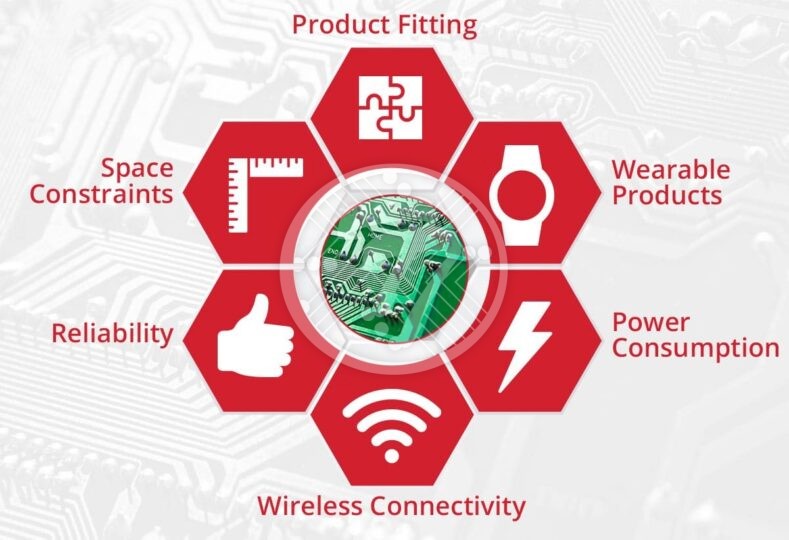
Here is how some of the challenges commonly associated with IOT can be overcome with smart PCB solution:

Space Constraints

When you have to fit the functionality of perhaps a smart phone into the size of a watch, that you have to fight for every inch, is a given. What can help solve this ever-growing space issue is Rigid flex as well as High Density Interconnect PCBs also popularly referred to as HDI PCBs. They allow for dense component placement that saves precious space. Also with rigid flex PCBs, you can fit the smallest of spaces opening up a world of possibilities when it comes to mobile devices. The added advantages that accrue with them include:

  • Reduced design limitation
  • The possibility of denser circuitry
  • Suitability for use in harsh environments
  • High tensile strength
  • Light weight- in fact they can offer weight savings of up to ninety five percent.
  • Greater resistance
  • Improved speed and reliability
  • Cleaner circuit route- HDI boards offer versatile routing options. Additionally, designers can replace through-holes with microvias, which go a long way in improving signal integrity.
  • Cost efficiency- A reduced need for layering lead to a product along with the smaller size also lead to evident advantages in cost.

In fact, Industry leaders focus on combining flex and HDI strategies to create designs that are both appealing as well as offer a whole lot of efficiency. The combination of the two also offers high tensile strength, as also the creation of electronics that are suitable for tough environments. They also go a long way in improving signal quality as well as reducing thermal stress.

Product fitting

Virtual prototyping can go a long way in keeping the design in sync with the IOT form that it is meant for. Often PCB designs would also need to make use of non-traditional materials such as mesh or plastic that will aid functionality.

Wearable products

The thing with wearable tech products is that the PCB design will need to budget for human body temperature, movement as well as moisture. To overcome this challenge smart PCB manufacturing relies on thorough simulation tests. The design needs to accommodate these aspects, as also allow sufficient cooling as soon as possible.

Power consumption

With IOT devices in constant communication with their networks, a strong focus on battery life and power integrity is a must have. The PCB design, therefore, needs to keep energy usage within the individual circuit blocks within a tight budget. Thorough testing can go a long way in overcoming the challenge of high power consumption.

Wireless Connectivity

IOT PCB has the added requirement of providing wireless internet access. This in turn requires installing the right wireless modules and RF Circuit components. Keeping the network speed, power consumption and any security issues in mind will help choose the right components and mitigate the challenges.

Reliability

With IOT devices being used in harsh environments, ensuring reliability and durability is a huge challenge. This can be tackled by using a whole lot of simulation software to test the PCB design under various conditions. In fact it is proper testing as well as working in cohesion with other designers that will ensure that the PCB works reliably under difficult situations.

One of the challenges of IOT is also the transition between the mechanical and the electronic; between the product itself and its PCB form, especially as newer and smaller IOT devices rule the roost. What can come in handy to achieve this is a close collaboration between the designers and engineers through out the design process.

With the industry growing by leaps and bounds, while there is going to be a whole lot of individualization in designs, the fact also is that there will be a lot of common requirements that could allow for some design protocols to emerge. With the development and sophistication in PCB designs the challenges are slowly but surely to get mitigated. The future certainly is one that will be fuelled with technology and innovation- a part that smart PCB manufacturing can play to the hilt. There is no doubt about the fact that approaches to PCB Design will continue to evolve at a rapid pace and that maximizing reliability and reducing errors will be the clarion call for all PCB designers.

At Technotronix, we are fully equipped to handle your PCB manufacturing requirements. With over 4 decades of experience in PCB manufacturing as well as assembling PCBs with differing levels of complexities, we follow industry best practices to ensure we deliver cutting-edge products. Our team of experts and state-of-the-art equipment ensures that all our PCBs meet the industry standards of quality and testing. It is our vast portfolio of satisfied clients that stand as the biggest testimony to our success. In case if you have any questions, please feel free to contact us via email at [email protected]

Expand the lifetime of your electronic device using flex pcb

By | Date posted: | Last updated: April 19, 2023
flex-pcb-1

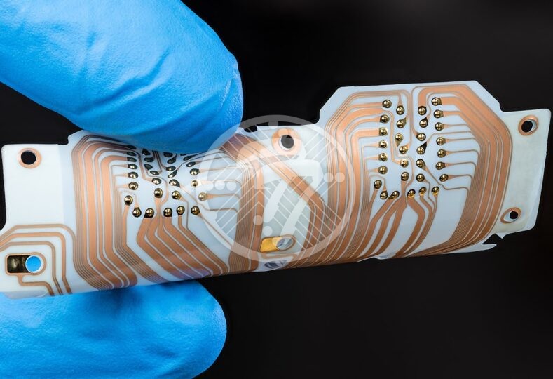
There would be very few takers wanting to build a device to fit the circuit board; most would prefer to design circuitry to fit the device. This is the exact reason why flex and rigid flex circuits are gaining increasing acceptance. They offer multiple advantages both in terms of a new project or even if you want to re-engineer an old one.

Flex PCBs find application in a number of electronic devices, hard disc drives and desktop printers. They are also used extensively in the following industries:

  • Communications
  • Consumer Electronics
  • Automotive
  • Medical
  • Aerospace
  • Military
  • Transportation

Even though they are not a new invention, they are increasingly being used for their versatility in design. They are known to unlock both functional advantages as well as cost savings for manufacturers.

Here are some of the key advantages of using flex PCB:

Reliability and increased life span of your electronic device

With both flex and rigid-flex PCB, the number of interconnections required are significantly reduced. What this in turn means is that there are fewer solder joints, contact crimps as well as connectors. Fewer interconnectors means that there are fewer sources of failure and hence greater reliability and increased life span of the device. The flexbility of the circuit also works towards improving shock performance.

flexbility in packaging

A Flexible PCB Board ensures that there is space saving as also more efficient use of space. What this means is that multiple circuit boards, connectors etc. can be replaced with a single unit. Typically it is seen that flex designs occupy 10% of the weight and space occupied by wired solutions. Fewer parts also create less supply chain risk as well as reduced maintenance requirement.

Improved Capability

 Flex systems are known for their superior performance. They accept any component or connector that works with a rigid PCB, besides working with direct solders, crimped contacts and the like. Besides, flexble circuits are not impacted by harsh environments, including high temperatures. They are also resistant when it comes to exposure to chemicals, radiations and UV.

Cost Efficient

 With lower material requirements, what a flexble circuit board also ensures is lower shipment costs. Also with fewer parts and simple installation the assembly costs are lower. Also with increased reliability comes cost saving on account of longer lasting products.

Also checkout: Flex Printed Circuit Board Cost

Precautions in using Flex PCBs

While a flexble printed circuit comes with a whole lot of advantages, it is important to keep some precautions in mind so that the circuit functions reliably.

There are some features that a rigid PCB can incorporate that a flex PCB must avoid. Primary among them being those that cause discontinuity in the bent areas. A via placed in the bent zone, for example can cause discontinuity. Additionally, conductor width or direction must not be changed in the bent area. An optimum flex-circuit design maintains a uniform width for all conductors. Also, a change in the direction of the conductor in the bend area needs to be avoided.

It is also important not to stack conductors on multiple layer boards. It is also prudent to not have sharp inside corners on the circuit outline as it can cause tears.

Some other areas to pay attention to include the fact that heat should not overstress the circuit. A heat gun can produce high enough temperatures to blister a circuit and hence its use should be avoided. Also, rigid temperature profiles need to be avoided when it comes to reflow flex PCBs.

Wide conductors are known to tolerate bending more than small ones so it is a good idea to widen small conductors in the bend area, even though the widening should be gradual. Also flex circuits with multiple layers are thicker. Often times though the combination of deep plated barrels with the added thickness leads to issues. It is therefore advisable to place vias in areas that have little or no bending or at least in areas that have least amount of bending.

As a standard practice it is also good to place fillets on via pads. They tend to eliminate stress points that have the potential of resulting in cracks.

It is also advisable to consult the Rigid flex PCB manufacturer during the design phase itself as that can lead to finding the most efficient solution that will work for your unique design.  With modern software programs complex 3D designs can be accommodated thereby allowing engineers to stack and test flex parts in layers. This in turn reduces the time and costs associated with testing. Modern 3D modeling software helps developers as well as fabricators to align their expectations as also to speed up the entire process.

With the above precautions in place you will be able to use your flex PCB to numerous advantages including giving your electronic products a whole new lease of life.

At Technotronix, we are fully equipped to handle your PCB manufacturing requirements. With over 4 decades of experience in rigid-flex PCB manufacturing as well as assembling PCBs with differing levels of complexities, our team of experts and state-of-the-art equipment ensures that all our PCBs meet the industry standards of quality and testing. In case if you have any questions, please feel free to contact us via email at [email protected].

PCB Conformal Coating vs PCB Encapsulation – Which one would you Choose?

By | Date posted: | Last updated: February 15, 2023
PCB Encapsulation

With the rapid growth in the electronics industry, the use of PCB is also growing exponentially. Its use in different applications however means that the PCB is subject to different environmental conditions. In places where the PCB is subject to moisture or harsh chemicals, performance can be of concern. It is therefore imperative that the PCB be coated to protect it from environmental conditions. This protection can be offered by way of either conformal coating or potting or by way of encapsulation.

Properties of PCB Potting and PCB Encapsulation:

Potting as well as encapsulation resins go a long way in offering a high level of protection for the PCB. In fact, encapsulation offers both electrical properties as well as mechanical protection. This high level of protection is ensured by way of a mass of resin surrounding the entire unit. This is far more substantial when compared to conformal coating. In fact, potting along with encapsulation offer fool proof protection. However potting and encapsulation resins need to be tested in a number of environments, so that their specifications and suitability for use can be determined. These tests typically involve exposing them to controlled atmospheric conditions over a period of time. The dimensions, weight and appearance of the resin is seen before and after the tests to check if any changes have occurred.

Properties of conformal coating PCB:

Besides potting and encapsulation resins, conformal coating can also be done in order to protect the PCB. This is done by applying it as a thin film. Since the film takes to the contours of the board, it does not cause any dimensional changes or add to the weight significantly. This in fact acts as a big advantage in favour of conformal coating as it lends itself easily to portability of the device. Tests, however, need to be conducted to evaluate the electrical and mechanical performance of the film in the applicable environment. The film needs to be tested in conditions such as humidity, temperature and more in order to determine the suitability of the film in such atmospheric conditions. Check out the guide on how Conformal Coating becoming a core driver to PCB Fabrication.

Application area of conformal coating & PCB potting

Both Conformal Coating as well as encapsulation and potting are available in different variants that make them suitable for particular applications. For standard conditions most, conformal coatings as well as potting and resin encapsulation work well. However, if the conditions are harsh, the choice of coating will vary. For example, acrylic coating works well in conditions where there is sustained exposure to UV light. However acrylic coating may not work well in conditions where the humidity levels are high. In such conditions, a Non-VOC Coating would work far better.

In cases where there is likely to be a lot of mechanical stress or where environmental conditions are harsh, optimum performance of the device will be obtained through the use of potting and encapsulation resins. Silicon resins or polyurethane resins are known to offer a greater degree of flexibility. In fact, polyurethane resins are preferred where temperatures are particularly low. They are also ideal for conditions where the device is immersed in water. Epoxy resins are preferable where exposure to chemicals is high.

Final words on Conformal coating vs potting:

Clearly therefore the choice of coating has a lot to do with the physical environment in which the device operates. While conformal coating scores on parameters such as ease and speed of processing, potting and encapsulation resins are preferable where climatic conditions are harsh. Conformal coating is also preferable where miniaturisation and portability of the device is essential. With both offering their distinct advantages, it is essential therefore to conduct a thorough evaluation of your unique requirements before coming at a decision with regard to the coating.

Technotronix is a skilled and experienced professional in providing apt PCB layout and PCB fabrication service. Our strong team of researchers and technical experts have made it possible to provide an effective lamination solution for your PCB project. Be it high frequency laminates, shrinking hole to hole pitch, exotic vias structures, multiple lamination cycle, lead free or halogen free solder assembly with strict environmental security considerations and high operating temperature are some of the highlights to our tough laminate technology implementation. You can drop an email to [email protected] or give us a call at 714/630-9200 to solve your queries or to get a quote.

The effects of ESD (Electrostatic discharge) on PCBs

By | Date posted: | Last updated: January 18, 2023
PCB Manufacturing

What is ESD?

Electrostatic Discharge or ESD as it is commonly called, occurs when two objects with different charges come close, so that the dielectric between them is broken. The common form of ESD that all of us are familiar with is lightning. Ever so often we could feel little sparks from a wool blanket, for example, which is once again a result of ESD.

How does ESD affect PCB?

When a PCB comes close to any object that has an opposite charge, it is subject to ESD. If the two come in contact, voltage is discharged and a massive voltage spike is created. Once the spike dissipates, electromagnetic fields are generated. It is therefore important to minimize the effect of the discharge. This is typically referred to as an PCB ESD Protection.

With modern chipsets having little tolerance for high voltage, an ESD event can as much as totally ruin the IC. The impact of ESD needs to therefore be factored in the design process of the PCB, as later it could lead to a host of redesigning to fix issues.

ESD can exist in many forms. While it typically requires several thousand volts for ESD to be felt by a person, even a small discharge can ruin semiconductors if the part is in the path of the ESD.
In turn this damage can be latent or catastrophic.

Catastrophic Damage:

This refers to the permanent damage to the device’s circuitry and can be detected using a performance test.

Latent damage:

This is said to occur when a device is partly degraded on account of being exposed to ESD yet continues to run even though its lifetime behavior is likely to be affected making the device unreliable.

Costly Effects Of ESD

While a catastrophic failure can be detected at an early manufacturing stage, it may not turn out to be as costly as a latent damage since it isn’t normally detected easily. As the product passes the regular inspection, latent failures can prove to be extremely costly besides impacting the company’s reputation.

What causes ESD?

ESD can be caused by a number of seemingly ordinary activities. A simple activity such as plugging in a cable can lead to a discharge. It is therefore important to protect your PCB from external connections as plugging in or pulling out a cable can expose the devise to the risk of ESD. There are, therefore, a number of precautions that can be taken to protect your PCB from the risk of ESD. Common precautions include:

  • Using a copper land or pad to attach connectors
  • Keep the pad separate from the PCB ground
  • Use a Transient Voltage Suppressor to protect the board

It is also prudent to establish and identify an ESD Protected Area, which is a clearly demarcated space within which all surfaces, objects, people and ESD Sensitive Devices (ESDs) are kept at the same potential. Typically all surfaces are linked to the ground. The area also needs to be identified with a clear signage and should allow access to only trained personnel. Periodic checks of installed products are mandatory within the area while all non-essential insulators need to be removed. It is also important to identify ESD Sensitive items as also to provide adequate ESD Control training to the staff to ensure that ESD control procedures are followed. The staff needs to be aware of the threat of ESD as also the ways and means of controlling static electricity.

PCB Layout to prevent Electrostatic Discharge

Apart from this, a whole lot of PCB Layout practices can go a long way in protecting PCB. These include:

Remove circuit loops:

Loops can lead to unwanted current. This in turn affects performance as unwanted current spikes can enter any loop. Due care therefore needs to be taken to ensure there are no loops.

Utilize ground plane layers in the printed circuit board:

Using a ground plane within a circuit board can go a long way in helping to reduce loops and therefore unwanted current.

Reduce line lengths:

Reducing line length in effect reduces the radiated energy received and therefore reducing the spikes from electrostatic discharges.

Reduce parasitic inductance:

Protection circuits can only work effectively if parasitic inductance levels are low. In turn parasitic inductance can be reduced by keeping the line lengths short.

Avoid running sensitive tracks near the extremity of the PCB:

The extremities of the board are more likely to pick up static discharge. It is therefore prudent to keep sensitive lines away from the extremities.

With electronic circuitry becoming increasingly smaller, the sensitivity to ESD is on the rise. What therefore also increases is the need for proper ESD protection.

Technotronix offers Electronics Manufacturing Service with combining state-of-the-art technology and advanced engineering to deliver unparalleled quality and service. Our prolonged goal is to serve our customers with electronic telecom solutions for development in telecommunication industry and to create advanced IT applications for our customers globally. To acquaint with Technotronix, reach us at [email protected] to get more information about PCB Manufacturing services for electrical telecom applications or prototypes!