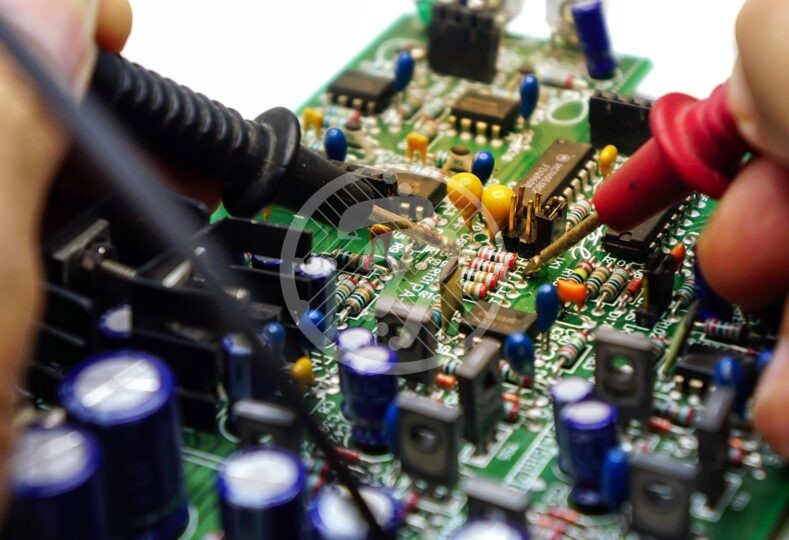
Creative Exposures in Testing the Circuits

The thumb rule for the growth of any OEM’s or PCB Fabricators or EMS providers is delivering quality printed circuit boards to help the customers get a quick turnaround. Deciding upon the method and technique of testing is the crucial step to move ahead with stringent inspection and quality check for maintenance, manufacturing and development in the assembly and fabrication process. There are various standard types of testing, which must be performed on printed circuit boards before and after the components are mounted on circuit board.
Flying Probe PCB testing:
When the printed circuit board has a complex layout and is manufactured in low volume, then the best testing solution is flying probe testing. Flying probe method has become more popular due to the development in the latest technology and increase in demand of PCB Prototyping Services. Whereas, when the layout is simple, but the volume of manufacturing is high, then the best testing solution is in-circuit (IC) testing. The important purpose behind these types of testing methods is to eliminate maximum fault coverage, higher beneficial production test, cost efficiency and minimize field failures.
The foundation of flying probe testing technique emphasizes mainly on increasing the improved access power, testing speed and cover greater fault coverage area. Flying probe is an ideal technique due to its low evolution costs, compactness and low evolution time. While testing the design, it is essential to consider the board, the devices on it, and the testing equipment’s capabilities. The major development and testing required is in the electrical circuit and mechanical path that significantly rectifies the speed.
When printed circuit boards have less compatibility, one of the major reasons is damaged internal circuit path and these results in many component failures which can be detected easily by using in-circuit testing technique. As for the high complexity board there are some shortcomings i.e., long programming is needed, which is more tedious, cumbersome for which in IC testing, the power signal is activated to check voltage levels and resistance measurements at different nodes of the board.
In-circuit test is used to detect parametric failures, design related faults and component failures. It can easily detect the fabricating defects and is also easy to measure the value of a component when it is not in a circuit.
To overcome the few shortcomings in the in-circuit test, there is an optimal test methodology, i.e., PCB functional test, which is the best option for testing the device equipments as it has a higher fault coverage area, no longer programming is needed, fewer field returns, more reliable fixtures, and lower overall costs. Thus functional testing is the essential part for having quality assurance of electronic products.
One of the biggest challenges for testing engineers and their managers is keeping up to date with technology trends. By working on these methodologies and technologies, product quality will be better positioned in years to come with optimal test processes.
At Technotronix, we combine state-of-the-art technology with our advanced engineering to deliver unparalleled quality and service. With fast PCB prototyping and consistent delivery of high-quality PCBs, we offer a robust source of competitive advantage to our clients. With our four decades of experience, you can rest assured that we are cognizant of the industry best practices and will keep you ahead of the curve. Visit to know more about PCB prototyping service and feel free to contact us. Also, you can drop an email to us at [email protected].


