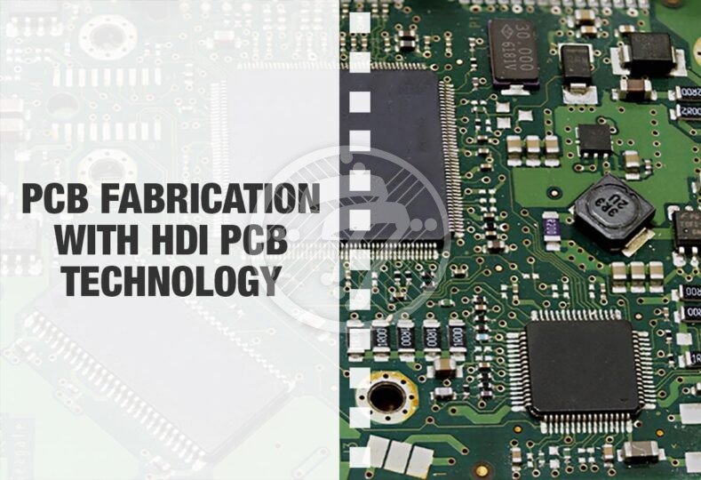
Enhance the Quality of PCB Fabrication with HDI PCB Technology!

If there is one trend when it comes to electronic devices, it has to be that of miniaturization. The size of electronic devices is shrinking and their complexity is on the rise. What this, in turn, means is the increase in demand of small PCBs. There is, therefore, a corresponding increase in the technology that can facilitate these small sized PCBs.
This is the exact reason why High Density Interconnect or HDI, as it is popularly called, is becoming increasingly relevant in today’s times.
What exactly is HDI technology?
Essentially, HDI technology is a result of evolution in component packaging that facilitates the construction of small boards that can have a large number of components per square inch. Simply put, an HDI PCB, therefore, has higher wiring density per unit area, as opposed to a conventional board. HDI printed circuit boards with one or all of the following:
- Microvias
- Blind vias
- Buried Vias
- Other microvias
- They also have built-up lamination and high signal performance.
In fact, it is the Microvias that have a huge role to play when it comes to the capabilities of HDI printed circuit boards. Since smaller vias can be close to each other, the board requirement is small. Also, space is easily freed up for additional components. With Microvias also having smaller aspect ratios that through-hole vias, the reliability quotient of HDI boards is far higher.
Importance of Using HDI PCB Fabrication
A typical PCB has one or two layers, while multilayer PCB can have up to 20 layers depending on their complexity. When it comes to HDI PCB, however, it could have as many as 40 layers which have densely mounted components, fine lines and micro vias. Some of the advantages of using HDI PCBs include:
- The ability to have several permutations and combinations when it comes to the layers.
- If you are looking for coreless designs, HDI PCBs come in handy
- With via-in pad, what you can also have is the maximum number of components in minimal number of layers.
- When it comes to mission-critical applications, The importance of HDI PCBs increase manifold.
- They offer the highest level of accuracy
- They have a better signal speed. The signal integrity is improved on account of shorter distance connections as well as lower power requirements.
- Some of the other performance improvements of HDI PCBs include stable voltage rail, lower RFI/EMI, distributed capacitance.
- It facilitates small cores and allows for fine drilling
- It also facilitates microvias
- It decreases power usage
- It is extremely cost effective
- It goes a long way in improving the overall performance of the device
- On account of the design efficiencies that HDI PCBs offer, it also allows for faster time-to-market, which is a significant source of competitive advantage in today’s times.
Applications of HDI PCBs
HDI PCBs are used in a wide range of industries, especially where miniaturization is prevalent. These would include digital devices, automobiles, aircrafts and more.
Another area where HDI PCB Fab finds a lot of application is to do with medical devices. With the need for small devices with high transmission rates, HDI PCBs fit the bill. This is especially true of implants but also of other medical equipment such as CT scans, MRI equipment and more.
The TechnoTronix advantage for HDI PCB Fabrication
At TechnoTronix, we have over 40 years of experience when it comes to manufacturing high quality PCBs. Our superior technical expertise ensures that we design custom made HDI PCBs for your bespoke requirements at competitive prices. We cater to a wide range of industries including but not limited to:
- Aerospace
- Defense
- Telecommunications
- Medical PCB Prototype
- Industrial PCB Prototype
- Renewable Energy PCB Prototype
- Rigid-Flex PCB Technology
If you are looking for best PCB fabrication services from product layout, manufacturing to warehousing and shipping, please explore our PCB fabrication services! We offer fast prototyping and consistent delivery of high quality products with quick turnaround times. We run extensive DFM tests to ensure that there are no costly errors later. The fact that we are an ISO 9001:2015 AS9100 Rev D company with unstinting focus on quality when it comes to PCB Fabrication ensures that you can rely on our services.


