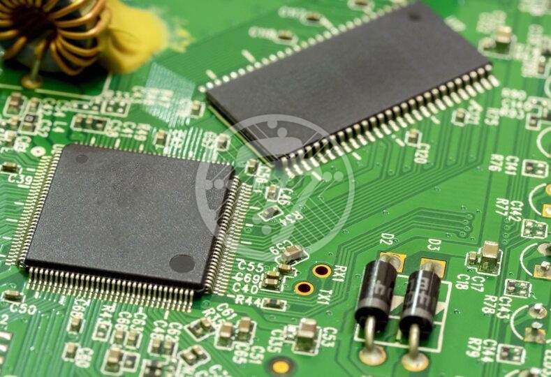
Increasing need of the fabrication and build out of PCB prototypes

A prototype is a sample, template or an initial testing release for any new idea to be worked into for providing the electronic solutions. The brainchild to printed circuit board concept into the market was in the early 1900’s. With regards to the backward integration sensed in major dominant businesses, there is a mark of growing demand and need of PCB Prototypes in all the major industries. The differentiating factor from that of other PCB fabricators are the varied kinds of PCB manufacturing services, time critical delivery of prototype and high quality assurance.
Apart from working on new concepts for prototyping, a complete turnkey with providing end to end solutions and a personalized approach to each PCB project acts as one of the significant drivers to generating a good customer base across the globe. Technology is at the heart of almost all the industries worldwide. The PCB Prototype demand is addressed in the dominant industries like aerospace, defense, telecommunication, medical, pharmaceutical and chemical.
PCB prototyping and PCB fabrication process
By using the Computer Aided Design (CAD) and Computer Aided Manufacturing (CAM), the OEM’s or PCB Manufacturer can commence smoothly for the PCB Fabrication process. The selection of the material meld or the fusion of different components to be made as per the requirement of the customers also reflects the success of the pcb layout and layout made by the technical experts. The advanced tools used at the time of prototyping are mainly for automated design analysis, algorithms and custom technical specimens.
After the copper coating is applied to the circuit board, the layout of the circuit will be printed on it and the unwanted copper will be ejected from the circuit. This will connect the circuit tracks on the board. On the board the holes are then drilled with a laser or a hard driller machine to connect the circuit tracks and hollow rivets are ejected into those holes to create an electrical flow in the layers of the circuit board. Different tactics and processes used to get a custom PCB prototyping are surface mount technique, reverse engineering of the electronic components, direct metallization, through-hole-technique and chip-on board technique.
The solder mask technique is then used for coating on complete circuit board. After the PCB is fabricated, its quality is being inspected to know the toughness and reliability of the prototype. The testing with regards to knowing the temperature profiling, issues pertaining to highly complex assemblies and to keep a check on resistance and density level at different nodes of the circuit board, there are many inspection techniques like thermal profiling, flying probe testing and functional testing.
TechnoTronix , one of the kingpins in offering tailor-made PCB prototypes has a flexible approach to use technical expertise and machines with moderate technologies which proves the reliability to load the project at the right time and economy. We have adopted flexibility to provide prototyping services with full or partial turnkey assembly as well as providing of prototyping service with consigned PCB assembly.
We strive to tender to a varied customization with optimal cost effective inventory management, effective procurement process of the components used in the PCB production, PCB Manufacturing with 2, 4 and 6 layered engineering, testing, and shipping PCB prototype’s for small run production. Thus our capabilities have outreached to expertise in PCB fabrication, prototyping, assembling, Layout and testing with high circuitry velocity, multi layering PCB and many features in a compact space.
Get a quick quote for PCB Prototype Fabrication!


