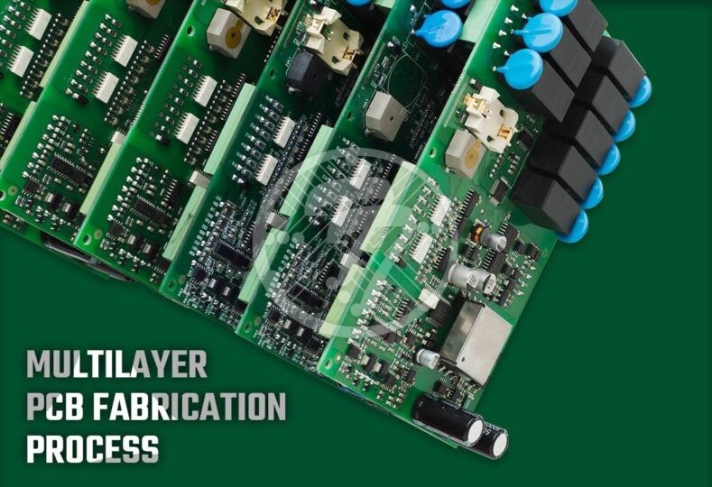
A Comprehensive Guide for Multilayer PCB Fabrication Process!

Multilayer PCB Fabrication is a complex process that requires expertise to master. Multilayer PCB assembly is quite a complicated task, there are several factors that affect the costing of Multilayer PCB assembly. But, as we are talking about the process of multilayer PCB Fabrication, here is a quick overview of the many aspects that make up the entire process of multilayer PCB Fabrication:
Checking design for manufacturability (DFM)
Once your PCB design is ready, you would be in a position to send the output files to a fabricator. What the fabricator will do is to make sure that the design works and that it is possible to build the board as per the design provided by you. With this check underway, the design output data will be used to create images. There are different tools that can be used by the fabricator such as:
-
Photoplotter
-
Direct Imaging technique
The fabricator will use either ultraviolet light through a process of photolithography or use a focused laser beam.
Inner layers for Multilayer PCB Fabrication
The inner layers of the PCB are typically made up of FR-4 material. The inner layer laminate is thus created, by bonding copper to the core material. The photoresist material is coated on the copper and one layer image from the PCB CAD data is exposed to the photoresist. The basic principle behind this, is that the exposed areas will harden while the unexposed ones, remain soft and pliant. The areas of unprotected copper can now etched away. Once the etching process is done, the hardened photoresist is removed.
The step now needs to be followed for each layer of the multilayer PCB fab. The next step is a process of thorough inspection through automated systems to ensure that there is no room for error.
Lamination in Multilayer PCB Fabrication
This step involves the use of prepeg, which is a sheet of fiberglass along with epoxy resin. The inner layers are then stacked along with prepeg to ensure there is alignment. The top and bottom prepeg layers are covered with copper foil. Now comes the final step of the lamination process whereby the entire unit is heated and the layers are fused into a circuit board.
Next comes the process of drilling and application of copper on the interior of the drilled holes.
Just as the inner layers were created, it is now time to add the top and bottom circuitry. The circuitry is then plated and covered with tin. It is time now to remove any remaining photoresist as well as etching away of extra copper and finally removing the tin.
Final touches
This step involves applying the solder mask. Post that, the choice of surface finish, silkscreen and markings are applied. A professional PCB fabricator is fully equipped to offer a wide range of surface finishes that the project demands.
Now comes a very important step in the process of multilayer PCB fabrication. This step is that of electrically testing the board. Post this there is a final inspection.
Clearly then the entire process involves a lot of expertise and precision. The litmus test of whether the PCB is built correctly begins at the design stage itself. With the use of proper design tools you can, in turn, ensure proper component placement, correct spacing etc. during fabrication. It is this expertise and precision that in turn results in boards that are:
- Light weight and small
- Are high on flexibility
- Lend themselves to high capacity and speed
Whether you are looking at a board with a few layers or complex boards up to 24 layers, what you will get is complete commitment to quality. In addition, we have some extremely stringent testing protocols that ensure that the boards never let you down!
At Technotronix, we have over 4 decades of experience in multilayer PCB fabrication. You can rely on our PCB design tools that, in turn, lead to that perfect PCB fabrication. An improper design can lead to a wide variety of issues such as imbalance.
Asymmetrical designs, for example, can lead to twisting or bows. It is extremely important, therefore, to go with a partner who understands these issues. Our experienced staff has a robust body of industry knowledge that ensures that you avoid costly mistakes later. Our superior engineering capabilities mean that each board matches your exact requirements and technical specifications. In case if you have any questions, please feel free to contact us via email at [email protected]


