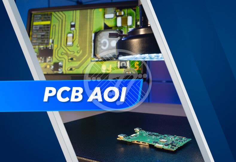
PCB AOI: Role of Automated optical inspection in PCB Manufacturing

The importance of testing in PCB manufacturing cannot be overstated. With PCBs being used for mission critical operations, the integrity & smooth functioning of the PCB is central to the efficacy of the device.
One of the important tests to check whether the PCB has any manufacturing faults is Automated Optical Inspection or what is popularly known as AOI.
What is Automated Optical Inspection (AOI)?
Essentially as its name suggests, it is a machine-based technique that checks the PCB for any potential defects such as:
- Surface Defects
- Dimensional Defects
- Component Placement Defects
With complex circuit boards and boards being manufactured in large quantities, manual checking becomes more & more difficult. AOI therefore has emerged as an important tool to check efficacy of the board at cost effective price points. Let us look at how it really works.
How exactly does AOI work?
Essentially the process works as follows. A first article PCB is manually inspected. Found good, it is established as a “golden” unit. The AOI then learns from this unit what the gold standard is, in terms of various aspects such as component placement, solder joints and more. This information is then stored in its database. The AOI system then compares each new board with this unit & alerts the operators in case of any inconsistency. The AOI system is equipped with high-resolution cameras, which capture a wide array of images, which come in handy for the comparisons. Different equipment works well for different kinds of inspection. So, while solder paste inspection is done by way of laser scanning, an assembly verification system relies on imaging.
Some of the methods that AOI makes use of, include:
Template matching – Simply put, this is a pixel-by-pixel method, where a small template is applied to a large inspection image. Normalized Cross Correlation is then calculated between the template & inspection image.
Object recognition – This method simply relies on a comparison between the ideal image & the captured image
Blob analysis – This involves separating the object from the background & then generating a blob by grouping object pixels.
Advantages of Automated Optical Inspection
AOI offers a wide range of advantages including but not limited to:
Miniaturization
With the increasing trend of miniaturization, the size of PCB components is constantly on the decline and component density is high. In such a scenario, AOI comes in extremely handy in checking for the positional accuracy of components. The advantage with AOI is that it can detect even small deviations in position eliminating chances of a defect.
Versatility
The big advantage with AOI is that it is useful not only in case of PCB fabrication but also in PCB assembly where it helps in checking for aspects such as soldering and polarity. The fact that AOI can be used at any stage makes it an ever so important tool when it comes to inspection efficacy
Programmable lighting
AOI makes it possible to configure light arrays within the inspection software. In turn, this is an invaluable tool that helps in a wide range of defect detection.
Data collection & Retrieval
AOI also helps in collection & retrieval of data which can take different formats such as image, data, text & more.
Cost Advantage
That AOI can help detect any manufacturing defects & save you from costly errors at a later date, makes it an extremely cost-effective process.
Let us also look at some of the defects that AOI can help check. These are on the spectrum of both Fabrication & Assembly.
Fabrication:
- Shorts
- Any violations in trace width
- Spacing violations
- Excess copper
- Missing component footprint pads.
- Drilled hole breakouts in PCB pads
Assembly:
- Inspection of solder paste.
- Finished solder joints.
- Checking the alignment of components
- Polarity indicators for component orientation.
- Marking of components
- Location of fiducials.
- Labels as well as other markings.
With the ability to capture a wide range of defects, little surprise then that AOI finds wide application. What it offers is both quick & accurate inspection of errors and thereby it ensures high quality PCBs. Right from bare circuit boards to the SMT Assembly line, its importance is therefore ubiquitous.
Technotronix is one of the leading PCB manufacturers in the USA, providing custom, lead-free and RoHS compliant PCB manufacturing solutions. Whether your requirement is for prototypes or large production runs, we have you covered.
Email us on [email protected] or call us on 714/630-9200 to solve your queries related to our standard PCB services.


