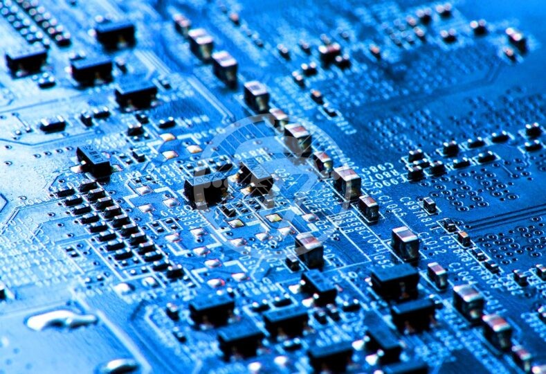
The modular approach for PCB Assembly and Design simplify the complexity for the Internet of Things Applications

Making a complex system, which has several components with interdependent functionalities based on different principles of electronics, can seem like an intimidating process. One needs to implement necessary business rules and technical principles and ensure synchronized communications. The complexity of the system is heightened by the number of functionalities and not necessarily the number of components of the system especially as one needs to keep track of the functionalities.
A modular approach for PCB Assembly goes a long way in simplifying complexity Making. Quite simply, modular Making means splitting up the seemingly complex design into small modules. You could compare it to Making a building which seems quite complex when finished, but which essentially requires breaking down the building plan into sub units and working on each of them independently. Essentially then modular Making implies splitting the system into sub modules and following an object-oriented programming where each module is independent of others and yet all modules work coherently together. To work on a modular approach, however, it is essential to identify the sub modules at the outset. This can be done by following these simple steps:
- Identify a functional sub system which can qualify as a module.
- Find all the components that go in to forming the sub module.
- Find the inputs and outputs of the module.
Basis this it is important to draw a diagram of how the components work together. Often at this stage, you may be able to break down the modules into smaller sub modules.
Adopting a modular design strategy also goes a long way in saving you from the monotony of Making the same kind of systems again and again. With the ability to reuse your PCB Layout you will be able to save time, energy and money, no mean feat! In fact, using a modular design for PCB goes a long way in reducing PCB manufacturing cost.
Below are some of the other advantages of utilizing a Modular PCB Design:
-
Ensuring an optimized workflow
– Most IoT things include predictable components. By using a modular approach, you can use the design elements with small changes to fit different requirements. It will be a lot easier to change the existing board than creating a fully new one.
-
Testing
– With unique boards for different products, what also becomes difficult is to test each of them independently. In the modular approach, however, with designs close to each other, testing them is far easier as also far more error free.
-
Marketing
– It is also far easier to market products that have a standardized design as systems engineers would already know how they work. This is as against developing a new design program which the systems engineers will need to check each time. Also with project time dramatically shortened, the time to market is far faster.
-
Cash flow optimization
– A standardized design process also leads to a significant cost saving as it requires far less man hours to develop the design. The time available at hand, can in turn be used to design boards for new products. Also, similar PCBs translate into lower manufacturing costs as lower labour as well as operational costs are achieved with shorter project time.
-
Less resource requirement
– The process is typically known to reduce material waste and thus optimize the overall process.
The process of modularization is made simpler through the use of many PCB tools.
Here are some commonly available tools for modular circuit board:
Drawing Tools
Drawing tools come in handy to place shapes on the board. You could also make use of the line drawing tool as it helps you draw connections to the other design aspects.
Custom Components
There is design software available that allow you to define custom components to be able to include it in the working schematic.
Notes
You can add notes to a drawn shape as it will help you record why a particular placement was made by you.
To-Do
You could create reminders for yourself through the use of a “to-dos” that can be made available throughout the project.
TechnoTronix is a leading manufacturer of high quality and lead-free pcb layout and PCB assembly service to the electronics manufacturers. Our qualified team of professionals use the modular approach for PCB Assembly and Layout to simplify the complexity for the Internet of Things Applications. To get more insights into the PCB assembly, layout and prototyping services, visit www.technotronix.us also You can drop an email to [email protected] or give us a call at 714/630-9200 to solve your queries or to get a quote.


